ADCMP603(Rev0) 데이터 시트보기 (PDF) - Analog Devices
부품명
상세내역
제조사
ADCMP603
(Rev.:Rev0)
(Rev.:Rev0)
Analog Devices

ADCMP603 Datasheet PDF : 16 Pages
| |||
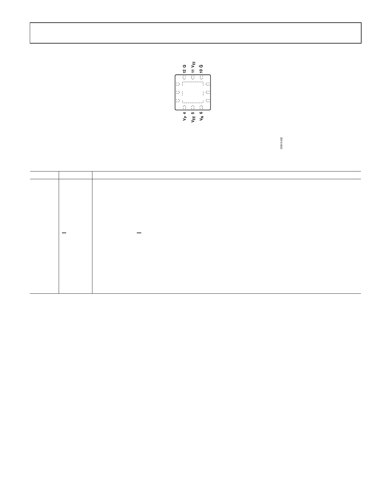
PIN CONFIGURATION AND FUNCTION DESCRIPTIONS
VCCO 1
VCCI 2
VEE 3
PIN 1
INDICATOR
ADCMP603
TOP VIEW
(Not to Scale)
9 VEE
8 LE/HYS
7 SDN
ADCMP603
Figure 3. ADCMP603 Pin Configuration
Table 5. Pin Function Descriptions
Pin No. Mnemonic Description
1
VCCO
Output Section Supply.
2
VCCI
Input Section Supply.
3
VEE
Negative Supply Voltage.
4
VP
Noninverting Analog Input.
5
VEE
Negative Supply Voltage.
6
VN
Inverting Analog Input.
7
SDN
Shutdown. Drive this pin low to shut down the device.
8
LE/HYS
Latch/Hysteresis Control. Bias with resistor or current for hysteresis adjustment; drive low to latch.
9
VEE
Negative Supply Voltage.
10
Q
Inverting Output. Q is at logic low if the analog voltage at the noninverting input, VP, is greater than the analog
voltage at the inverting input, VN, if the comparator is in compare mode. See the LE/HYS pin description (Pin 8)
for more information.
11
VEE
Negative Supply Voltage.
12
Q
Noninverting Output. Q is at logic high if the analog voltage at the noninverting input, VP, is greater than the
analog voltage at the inverting input, VN, if the comparator is in compare mode. See the LE pin description
(Pin 8) for more information.
Heat Sink VEE
Paddle
The metallic back surface of the package is electrically connected to VEE. It can be left floating because Pin 3, Pin 5,
Pin 9, and Pin 11 provide adequate electrical connection. It can also be soldered to the application board if
improved thermal and/or mechanical stability is desired. Exposed metal at package corners is connected to the
heat sink paddle.
Rev. 0 | Page 7 of 16
Share Link: