EVAL-ADCMP607BCPZ(RevB) 데이터 시트보기 (PDF) - Analog Devices
부품명
상세내역
제조사
EVAL-ADCMP607BCPZ
(Rev.:RevB)
(Rev.:RevB)
Analog Devices

EVAL-ADCMP607BCPZ Datasheet PDF : 14 Pages
| |||
Data Sheet
ADCMP606/ADCMP607
COMPARATOR PROPAGATION DELAY
DISPERSION
The ADCMP606/ADCMP607 comparators are designed to
reduce propagation delay dispersion over a wide input overdrive
range of 5 mV to VCCI − 1 V. Propagation delay dispersion is the
variation in propagation delay that results from a change in the
degree of overdrive or slew rate (that is, how far or how fast the
input signal exceeds the switching threshold).
Propagation delay dispersion is a specification that becomes
important in high speed, time-critical applications, such as data
communication, automatic test and measurement, and
instrumentation. It is also important in event-driven applications,
such as pulse spectroscopy, nuclear instrumentation, and
medical imaging. Dispersion is defined as the variation in
propagation delay as the input overdrive conditions are changed
(Figure 15 and Figure 16).
The device dispersion is typically 2.3 ns as the overdrive varies
from 10 mV to 125 mV. This specification applies to both
positive and negative signals because each device has very closely
matched delays for positive-going and negative-going inputs as
well as very low output skews.
500mV OVERDRIVE
INPUT VOLTAGE
10mV OVERDRIVE
VN ± VOS
DISPERSION
Q/Q OUTPUT
Figure 15. Propagation Delay—Overdrive Dispersion
INPUT VOLTAGE
1V/ns
10V/ns
VN ± VOS
DISPERSION
Q/Q OUTPUT
Figure 16. Propagation Delay—Slew Rate Dispersion
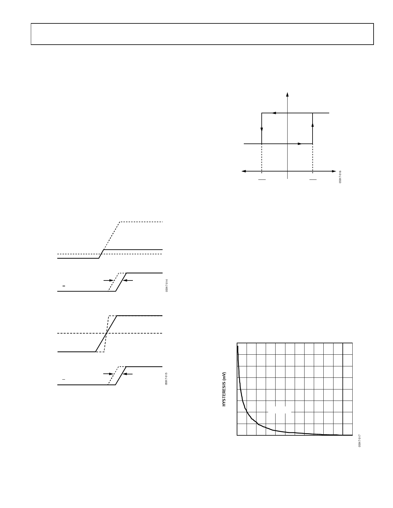
COMPARATOR HYSTERESIS
The addition of hysteresis to a comparator is often desirable in a
noisy environment, or when the differential input amplitudes
are relatively small or slow moving. Figure 17 shows the transfer
function for a comparator with hysteresis. As the input voltage
approaches the threshold (0 V, in this example) from below the
threshold region in a positive direction, the comparator switches
from low to high when the input crosses +VH/2, and the new
switching threshold becomes −VH/2. The comparator remains in
the high state until the new threshold, −VH/2, is crossed from
below the threshold region in a negative direction. In this manner,
noise or feedback output signals centered on 0 V input cannot
cause the comparator to switch states unless it exceeds the region
bounded by ±VH/2.
OUTPUT
VOH
VOL
–VH
0
2
+VH INPUT
2
Figure 17. Comparator Hysteresis Transfer Function
The customary technique for introducing hysteresis into a
comparator uses positive feedback from the output back to the
input. One limitation of this approach is that the amount of
hysteresis varies with the output logic levels, resulting in
hysteresis that is not symmetric about the threshold. The
external feedback network can also introduce significant
parasitics that reduce high speed performance and induce
oscillation in some cases.
This ADCMP607 comparator offers a programmable hysteresis
feature that can significantly improve accuracy and stability.
Connecting an external pull-down resistor or a current source
from the LE/HYS pin to GND, varies the amount of hysteresis in a
predictable, stable manner. Leaving the LE/HYS pin disconnected
or driving this pin high removes hysteresis. The maximum
hysteresis that can be applied using this pin is approximately
160 mV. Figure 18 illustrates typical hysteresis applied as a
function of the external resistor value, and Figure 8 illustrates
typical hysteresis as a function of the current.
400
350
300
250
200
150
100
VCC = 2.5V
50
0
50 100 150 200 250 300 350 400 450 500 550 600 650
HYS RESISTOR (kΩ)
Figure 18. Hysteresis vs. RHYS Control Resistor
Rev. B | Page 11 of 14
Share Link: