TDA8948J 데이터 시트보기 (PDF) - NXP Semiconductors.
부품명
상세내역
제조사
TDA8948J Datasheet PDF : 26 Pages
| |||
NXP Semiconductors
TDA8948J
4-channel audio amplifier
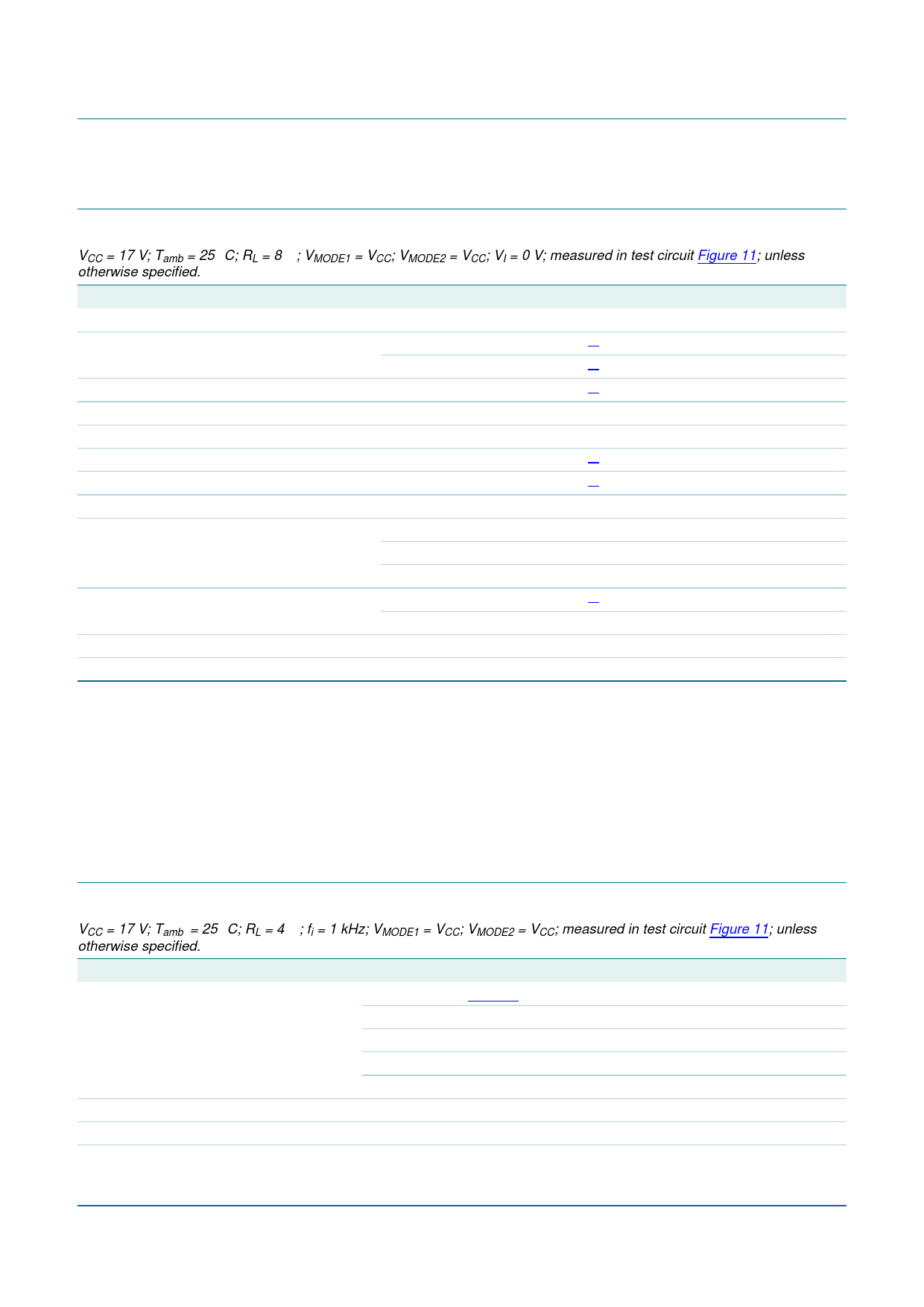
11. Static characteristics
Table 8. Static characteristics
VCC = 17 V; Tamb = 25 °C; RL = 8 Ω; VMODE1 = VCC; VMODE2 = VCC; VI = 0 V; measured in test circuit Figure 11; unless
otherwise specified.
Symbol
Parameter
Conditions
Min
Typ Max
Unit
Supply
VCC
supply voltage
operating
no (clipping) signal
[1] 9
[2] -
17
26
V
-
28
V
Iq
Istb
Output pins
quiescent current
standby current
VCC = 17 V; RL = ∞
-
[3] -
100 145
mA
-
-
10
µA
VO
output voltage
∆VO(offset)
differential output voltage offset
Mode selection pins
-
BTL mode
[4] -
[5] -
9
-
V
-
170
mV
VMODE1
voltage on pin MODE1
on mode
mute mode
standby mode
VCC − 2.0 -
4.5
-
0
-
VCC
V
VCC − 3.5 V
0.8
V
VMODE2
IMODE1
IMODE2
voltage on pin MODE2
current on pin MODE1
current on pin MODE2
on mode: channels 3 and 4
mute mode: channels 3 and 4
0 V < VMODE1 < (VCC − 3.5 V)
0 V < VMODE2 < (VCC − 3.5 V)
[6] VCC − 2.0 -
0
-
-
-
-
-
VCC
V
VCC − 3.5 V
20
µA
20
µA
[1] A minimum load is required at supply voltages of VCC > 22 V: RL = 3 Ω for SE and RL = 6 Ω for BTL.
[2] The amplifier can deliver output power with non-clipping output signals into nominal loads as long as the ratings of the IC are not
exceeded.
[3] With a load connected at the outputs the quiescent current will increase.
[4] The DC output voltage, with respect to ground, is approximately 0.5 VCC.
[5] ∆VO(offset) = |VOUT+ − VOUT−|
[6] Channels 3 and 4 can only be set to mute or on mode by MODE2 when VMODE1 > VCC − 2.0 V.
12. Dynamic characteristics
Table 9. Dynamic characteristics SE
VCC = 17 V; Tamb = 25 °C; RL = 4 Ω; fi = 1 kHz; VMODE1 = VCC; VMODE2 = VCC; measured in test circuit Figure 11; unless
otherwise specified.
Symbol Parameter
Conditions
Min
Typ
Max
Unit
Po(SE)
SE output power
THD
Gv
Zi
total harmonic distortion
voltage gain
input impedance
VCC = 17 V; see Figure 7
THD = 10 %; RL = 4 Ω
THD = 0.5 %; RL = 4 Ω
VCC = 20 V
THD = 10 %; RL = 4 Ω
Po = 1 W
-
-
6.5
8
-
W
-
6
-
W
-
12
-
W
-
0.1
0.5
%
25
26
27
dB
40
60
-
kΩ
TDA8948J_1
Product data sheet
Rev. 01 — 27 February 2008
© NXP B.V. 2008. All rights reserved.
9 of 26
Share Link: 