ADCMP609(RevPrA) 데이터 시트보기 (PDF) - Analog Devices
부품명
상세내역
제조사
ADCMP609
(Rev.:RevPrA)
(Rev.:RevPrA)
Analog Devices

ADCMP609 Datasheet PDF : 16 Pages
| |||
Preliminary Technical Data
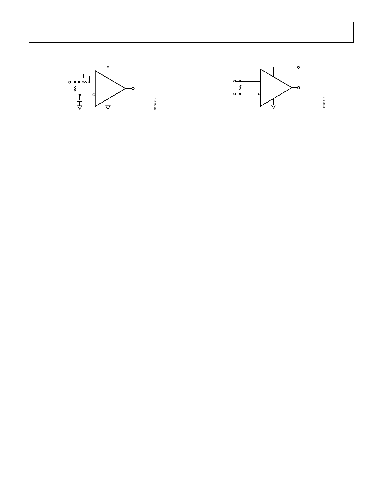
APPLICATION INFORMATION
POWER/GROUND LAYOUT AND BYPASSING
The ADCMP608 and ADCMP609 comparators are high speed
devices. Despite the low noise output stage, it is essential to use
proper high speed design techniques to achieve the specified
performance. Because comparators are uncompensated
amplifiers, feedback in any phase relationship is likely to cause
oscillations or undesired hysteresis. Of critical importance is the
use of low impedance supply planes, particularly the output
supply plane (VCCO) and the ground plane (GND). Individual
supply planes are recommended as part of a multilayer board.
Providing the lowest inductance return path for switching
currents ensures the best possible performance in the target
application.
It is also important to adequately bypass the input and output
supplies. A 0.1 μF bypass capacitor should be placed as close as
possible to each VCC supply pin. The capacitor should be
connected to the GND plane with redundant vias placed to
provide a physically short return path for output currents
flowing back from ground to the VCC pin. High frequency
bypass capacitors should be carefully selected for minimum
inductance and ESR. Parasitic layout inductance should also be
strictly controlled to maximize the effectiveness of the bypass at
high frequencies.
TTL-/CMOS-COMPATIBLE OUTPUT STAGE
Specified propagation delay performance can be achieved only
by keeping the capacitive load at or below the specified mini-
mums. The outputs of the ADCMP608 and ADCMP609 are
designed to directly drive one Schottky TTL or three low power
Schottky TTL loads or equivalent. For large fan outs, buses, or
transmission lines, an appropriate buffer should be used to
maintain the excellent speed and stability of the part.
With the rated 15 pF load capacitance applied, even at 2.5 V
VCC, more than half of the total device propagation delay is
output stage slew time. Because of this, the total prop delay will
decrease as VCCO decreases and instability in the power supply
may show up as excess delay dispersion.
This delay is measured to the 50% point for whatever supply is
in use, so the fastest times will be observed with the VCC supply
at 2.5 V, and larger values will be observed when driving loads,
that switch at other levels. Overdrive and input slew rate
dispersions are not significantly affected by output loading and
VCC variations.
The TTL/CMOS-compatible output stage is shown in the
simplified schematic diagram of Figure 12. Because of its
inherent symmetry and generally good behavior, this output
stage is readily adaptable for driving various filters and other
unusual loads.
ADCMP608/ADCMP609
VLOGIC
A1
Q1
+IN
AV
–IN
OUTPUT
A2
Q2
GAIN STAGE
OUTPUT STAGE
Figure 13. Simplified Schematic Diagram
of TTL/CMOS-COMPATIBLE Output Stage
USING/DISABLING THE LATCH FEATURE
The latch input of the ADCMP609 is designed for maximum
versatility. It can safely be left floating or pulled to TTL high for
normal comparator operation with no hysteresis, or it can be
driven low by any standard TTL/CMOS device as a high speed
latch.
In addition, the pin can be operated as a hysteresis control pin
with a bias voltage of 1.25 V nominal and an input resistance of
approximately 7000 Ω. This allows the comparator hysteresis to
be easily and accurately controlled by either a resistor or an
inexpensive CMOS DAC.
Hysteresis control and latch mode can be used together if an
open drain, a collector, or a three-state driver is connected in
parallel to the hysteresis control resistor or current source.
Due to the programmable hysteresis feature,the logic threshold
of the latch pin is approximately 1.1 V regardless of VCC.
OPTIMIZING PERFORMANCE
As with any high speed comparator, proper design and layout
techniques are essential for obtaining the specified
performance. Stray capacitance, inductance, common power
and ground impedances, or other layout issues can severely limit
performance and often cause oscillation. The source impedance
should be minimized as much as is practicable. High source
impedance, in combination with the parasitic input capacitance
of the comparator, will cause an undesirable degradation in
bandwidth at the input, thus degrading the overall response.
Higher impedances encourage undesired coupling.
Rev. PrA | Page 9 of 16
Share Link: