MAX914 데이터 시트보기 (PDF) - Maxim Integrated
부품명
상세내역
제조사
MAX914 Datasheet PDF : 12 Pages
| |||
40ns, Low-Power, 3V/5V, Rail-to-Rail
Single-Supply Comparators
ABSOLUTE MAXIMUM RATINGS
Power Supply Ranges
Supply Voltage (VCC to GND)...........................................+6V
Differential Input Voltage .......................-0.3V to (VCC + 0.3V)
Common-Mode Input Voltage to GND ..-0.3V to (VCC + 0.3V)
LE Input Voltage (MAX9141 only) .........-0.3V to (VCC + 0.3V)
SHDN Input Voltage (MAX9141 only)....-0.3V to (VCC + 0.3V)
Input/Output Short-Circuit Duration to
VCC or GND .....................................................Continuous
Continuous Power Dissipation (TA = +70°C)
5-Pin SC70 (derate 3.1mW/°C above +70°C) .............247mW
5-Pin SOT23 (derate 7.1mW/°C above +70°C)...........571mW
8-Pin SOT23 (derate 9.1mW/°C above +70°C)...........727mW
8-Pin SO (derate 5.9mW/°C above +70°C)..............470.6mW
14-Pin TSSOP (derate 9.1mW/°C above +70°C) ........727mW
14-Pin SO (derate 8.33mW/°C above +70°C)..........666.7mW
Operating Temperature Range ...........................-40°C to +85°C
Storage Temperature Range .............................-65°C to +150°C
Lead Temperature (soldering, 10s) .................................+300°C
Stresses beyond those listed under “Absolute Maximum Ratings” may cause permanent damage to the device. These are stress ratings only, and functional
operation of the device at these or any other conditions beyond those indicated in the operational sections of the specifications is not implied. Exposure to
absolute maximum rating conditions for extended periods may affect device reliability.
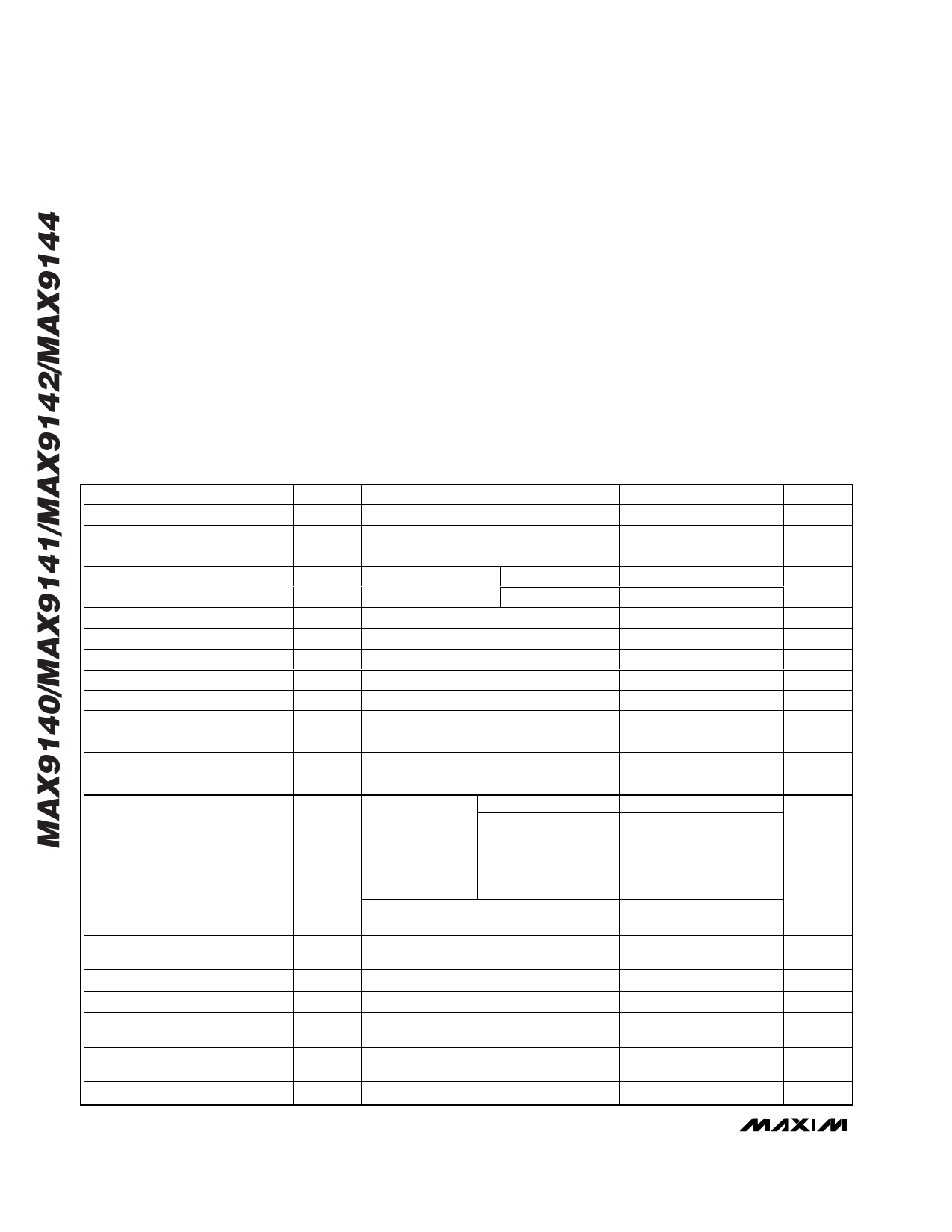
ELECTRICAL CHARACTERISTICS
(VCC = 5V, VCM = 0, SHDN = LE = VCC (MAX9141 only), CL = 15pF, TA = TMIN to TMAX, unless otherwise noted. Typical values are
at TA = +25°C.) (Note 1)
PARAMETER
SYMBOL
CONDITIONS
MIN TYP MAX UNITS
Operating Supply Voltage
VCC (Note 2)
2.7
5.5
V
Input Voltage Range
VCMR (Note 3)
-0.2
VCC +
0.2
V
Input Offset Voltage
Input Hysteresis
Input Bias Current
Input Offset Current
Common-Mode Rejection Ratio
Power-Supply Rejection Ratio
VOS
VHYST
IB
IOS
CMRR
PSRR
(Note 4)
(Note 5)
(Note 6)
VCC = 5.5V (Note 7)
2.7V ≤ VCC ≤ 5.5V
TA = +25°C
TA = TMIN to TMAX
0.5
2
4.5
1.5
90
320
8
120
80
800
80
750
mV
mV
nA
nA
µV/V
µV/V
Output High Voltage
VOH ISOURCE = 4mA
VCC - VCC -
0.425 0.3
V
Output Low Voltage
VOL ISINK = 4mA
0.3 0.425
V
Output Leakage Current
ILEAK SHDN = GND, MAX9141 only (Note 8)
0.04
1
µA
MAX9141
165
275
VCM = VCC = 3V MAX9140/MAX9142/
MAX9144
150
250
Supply Current (Per Comparator)
Propagation Delay
ICC
tPD+,
tPD-
MAX9141
VCM = VCC = 5V MAX9140/MAX9142/
MAX9144
MAX9141 only, SHDN = GND;
VCC = VCM = 3V
VCC = 3V, VOD = 10mV
200
320
µA
165
300
12
30
40
ns
Differential Propagation Delay
dtPD VOD = 10mV (Note 9)
2
ns
Propagation Delay Skew
VOD = 10mV (Note 10)
2
ns
Logic Input Voltage High
VIH (Note 11)
VCC/2 +
0.4
VCC/2
V
Logic Input Voltage Low
VIL (Note 11)
VCC/2
VCC/2 -
0.4
V
Logic Input Current
IIL, IIH VLOGIC = 0 to VCC (Note 11)
2
10
µA
2 _______________________________________________________________________________________
Share Link: 