TS372C 데이터 시트보기 (PDF) - Unspecified
부품명
상세내역
제조사
TS372C Datasheet PDF : 5 Pages
| |||
TS372C,I,M
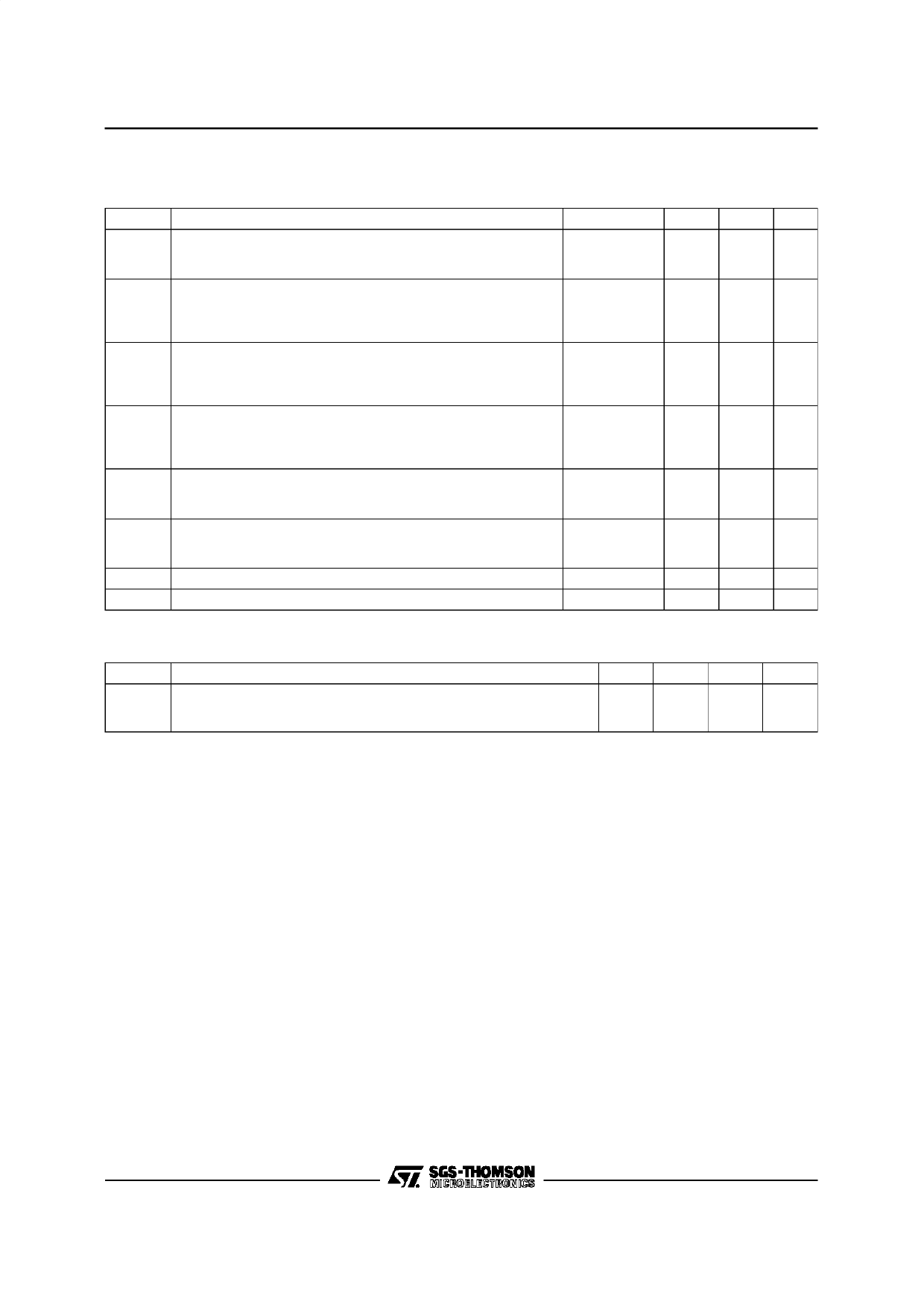
ELECTRICAL CHARACTERISTICS
VCC+ = 5V, VCC- = 0V, Tamb = 25oC (unless otherwise specified)
Symbol
Vio
Iio
Iib
Vicm
IOH
VOL
IOL
ICC
Parameter
Input Offset Voltage
Tamb = 25oC
(Vic
=
Vicm
min.)
-
(note
1)
Tmin. ≤ Tamb ≤ Tmax.
Input Offset Current - (note 2)
Tamb = 25oC
Tmin. ≤ Tamb ≤ Tmax.
TS372C
TS372I/TS372M
Input Bias Current - (note 2)
Tamb = 25oC
Tmin. ≤ Tamb ≤ Tmax.
TS372C
TS372I/TS372M
Input Common Mode Voltage Range
Tamb = 25oC
Tmin. ≤ Tamb ≤ Tmax.
TS372C
TS372I/TS372M
High Level
Tamb =
Output
25oC
Current
(Vid
=
1V)
Tmin. ≤ Tamb ≤ Tmax.
VOH = 5V
VOH = 15V
Low Level
Tamb =
Output
25oC
Voltage
(Vid
=
-1V,
IOL =
4mA)
Tmin. ≤ Tamb ≤ Tmax.
Low Level Output Current (Vid = -1V, VOL = 1.5V)
Supply Current (2 comparators) (Vid = +1V, no load)
Min.
Typ.
2
1
1
000ttootoVVVCCCCC+C++--2-22..255
0.1
100
6
45
0.3
Max. Unit
mV
10
12
pA
100
200
pA
150
300
V
nA
1
µA
mV
400
700
mA
0.75 mA
SWITCHING CHARACTERISTICS (VCC+ = 5V, Tamb = 25oC)
Symbol
Parameter
Min. Typ. Max. Unit
tre
Response Time (RL = 5.1kΩ connected to 5V, CL = 15pF - (note 3)
• 100mV input step with 5mV overdrive
• TTL level input step
ns
600
200
Notes : 1. The specified offset voltage is the maximum value required to drive the output down to 400mV or up
to 4V with RL = 100kΩ to VCC+.
2. Maximum values including unavoidable inaccuracies of the industrial test.
3. The response time which is specified is the internal between the input signal and the instant when the output signal crosses 1.4V.
3/5
Share Link: 