TDA9210 데이터 시트보기 (PDF) - STMicroelectronics
부품명
상세내역
제조사
TDA9210 Datasheet PDF : 19 Pages
| |||
TDA9210
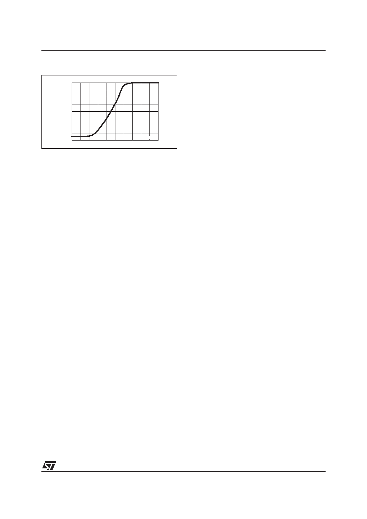
Figure 2.
Attenuation (dB)
0
-2
-4
-6
-8
-10
-12
-14
-16
0
1
2
3
VABL (V)
4
5
4.6 - Brightness Adjustment (8 bits)
Brightness adjustment is controlled by the I2C Bus
via Register 2. It consists of adding the same DC
voltage to the three RGB signals, after contrast ad-
justment. When the blanking pulse equals 0, the
DC voltage is set to a value which can be adjusted
between 0 and 2V with 8mV steps (see Figure 3).
The DC output level is forced to the ”Infra Black”
level (VDC) when the blanking pulse is equal to 1.
4.7 - Drive Adjustment (3 x 8 bits)
In order to adjust the white balance, the TDA9210
offers the possibility of adjusting separately the
overall gain of each channel thanks to the I2C bus
(Registers 3, 4 and 5).
The very large drive adjustment range (48 dB) al-
lows different standards or custom color tempera-
tures.
It can also be used to adjust the output voltages at
the optimum amplitude to drive the CRT drivers,
keeping the whole contrast control for the end-
user only.
The drive adjustment is located after the Contrast,
Brightness and OSD switch blocks, so it does not
affect the white balance setting when the BRT is
adjusted. It also operates on the OSD portion of
the signal.
4.8 - OSD Inputs
The TDA9210 allows to mix the OSD signals into
the RGB main picture. The four pins dedicated to
this function are the following:
– Three TTL RGB inputs (Pins 8, 9, 10) connected
to the three outputs of the corresponding OSD
processor.
– One TTL fast blanking input (Pin 11) also con-
nected to the FBLK output of the OSD processor.
When a high level is present on the FBLK, the IC
acts as follows:
– The three main picture RGB input signals (IN1,
IN2, IN3) are internally switched to the internal
input clamp reference voltage.
– The three output signals are set to the voltage
corresponding to the three OSD input logic
states (0 or 1). (See Figure 3).
If the OSD input is at low level, the output and
brightness voltages (VBRT) are equal.
If the OSD input is at high level, the output voltage
iasnVI2OCSDb,uws-hceornetrVoOlleSdDv=olVtaBgReT. + OSD and OSD is
OSD varies between 0 V to 4.9 V by 320 mV steps
via Register 7 (4 bits). The same variation is ap-
plied simultaneously to the three channels provid-
ing the OSD contrast.
The grey color can be obtained on output signals
when:
– OSD1 = 1, OSD2 = 0 and OSD3 = 1,
– A special bit (bit 5 or 6) in Register 9 is set to 1.
If R9b5 is set to 1, light grey is obtained on output.
If R9b6 is set to 1, dark grey is obtained on output.
In the case where R9b5 and R9b6 are set to 0, the
normal operation is provided on output signals.
4.9 - Output Stage
The overall waveforms of the output signal are
shown in Figure 3 and Figure 4. The three output
stages, which are large bandwidth output amplifi-
ers, are able to deliver up to 4.4 VPP for 0.7 VPP on
input.
When a high level is applied on the BLK input
(Pin 20), the three outputs are forced to ”Infra
Black” level (VDC) thanks to a sample and hold cir-
cuit (described below).
The black level (which is the output voltage out-
side the blanking pulse with minimum brightness
and no Video input signals) is 400 mV higher than
VDC.
The brightness level
programming register
(VBRT)
2 (see
is then obtained
I2C table 1).
by
The sample and hold circuit is used to control the
”Infra Black” level in the range of 0.5 V to 2.5 V via
Register 6 (in case of AC coupling) or Registers
10, 11, 12 (in case of DC coupling) .
This sampling occurs during an internal pulse
(OCL) generated inside the blanking pulse win-
dow.
Refer to “CRT cathode coupling” part for further
details.
5/19
Share Link: 