EM357 데이터 시트보기 (PDF) - California Eastern Laboratories.
부품명
상세내역
제조사
EM357
California Eastern Laboratories.

EM357 Datasheet PDF : 16 Pages
| |||
MeshConnect™ EM357 Module
TRANSCEIVER IC
The MeshConnect EM357 Module uses the Ember EM357 transceiver IC. This IC incorporates the RF transceiver
with the baseband modem, a hardwired MAC and an embedded ARM® Cortex™-M3 microcontroller, offering an
excellent low cost high performance solution for all IEEE 802.15.4/ZigBee applications.
For more information about the Silicon Laboratories EM357 IC, visit http://www.silabs.com
ADDITIONAL FLASH MEMORY
The MeshConnect EM357 Modules (ZICM357P2-2 and ZICM357P2-2C) incorporates an optional additional 1MB
external Flash memory for OTA program updates. The Flash memory communicates over the EM357’s second
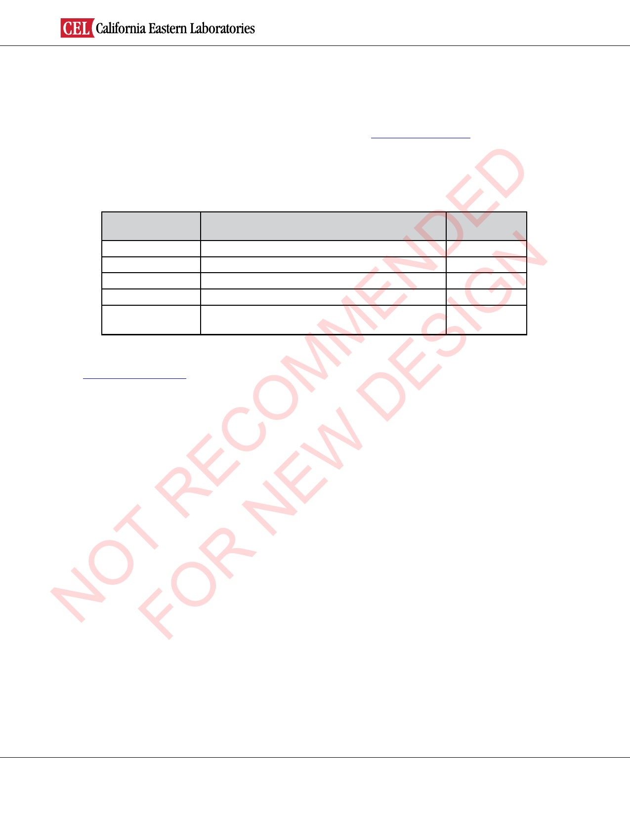
D serial controller using SPI. The Flash memory is wired to the following castellation pins:
E GPIO Name
PA0
D PA1
N N PA2
PA3
E IG WP
Function
SC2MOSI
SC2MISO
SC2SCLK
SC2nSSEL
Flash memory Write Protect line (has internal pull-up
resistor, but not connected to the EM357)
EM357 Module
Pin Number
3
4
5
6
2
The instruction set for the Flash memory is similar to the Micron M25PE80. Note: In order to achieve the specified
M S sleep current for the module, it is necessary to send a Deep Power-Down command to the Flash memory.
See http://www.micron.com for more information on the instruction set.
M E ANTENNA
The MeshConnect EM357 Module includes an integrated Printed Circuit Board (PCB) trace antenna. An optional
O D U.FL connector can be specified, providing connection to a 50-ohm external antenna of the user’s choice. However,
use of an external antenna is not covered by the module's certification; see Ordering Information on Page 1.
C For optimum antenna performance, the MeshConnect EM357 Module should be mounted with the PCB trace
E W antenna overhanging the edge of the host board. To further improve performance, a ground plane may be placed
on the host board under the module up to the antenna. The installation of an uninterrupted ground plane on a
E layer directly beneath the module will also allow you to run traces under this layer. CEL can provide assistance
R with your PCB layout.
N The PCB antenna employs an Inverted F-Antenna topology that is compact and highly efficient. To maximize
T range, an adequate ground plane must be provided on the host PCB. Correctly positioned, the ground plane on
the host PCB will contribute significantly to the antenna performance; it should not be directly under the Inverted
O R F-Antenna. The position of the module on the host board and overall design of the product enclosure contribute
to antenna performance. Poor design affects radiation patterns and can result in reflection, diffraction and/or
N O scattering of the transmitted signal.
F A few design guidelines to help ensure antenna performance:
• Never place the ground plane or route copper traces directly underneath the antenna portion of the module
• Never place the antenna close to metallic objects
• In the overall design, ensure that wiring and other components are not placed near the antenna
• Do not place the antenna in a metallic or metalized plastic enclosure
• Keep plastic enclosures 1cm or more away from the antenna in any direction
Page 4
Share Link: