FS6159-01 데이터 시트보기 (PDF) - AMI Semiconductor
부품명
상세내역
제조사
FS6159-01 Datasheet PDF : 15 Pages
| |||
FS6159-01
Auxiliary Motherboard Clock Generator/Buffer IC
1.0 Features
• Develops the peripheral clocks required for 2-way
and 4-way multi-processor clock-partitioned plat-
forms, including:
M Six buffered copies of the 66.67MHz 66REF ref-
erence input
M Twelve 33.3MHz PCI clocks, developed as a di-
vide-by-two of the 66REF reference input
M Two buffered copies of the 14.318MHz 14REF
reference input
M Two 48MHz clocks, generated by a PLL from the
14REF reference input
• Serial-bus interface control of all clock outputs
• Three clock management controls enable, disable
and tristate banks of clock outputs independently of
the serial interface
• Active-low PWR_DWN# signal allows shuts down the
PLL and disables outputs low
• Supports Test Mode and tristate output control to fa-
cilitate board testing
• Available in a 56-pin SSOP and TSSOP
Table 1: Clock Parameters
CLOCK
GROUP
CK66
PCI
REF
CK48
# SUPPLY SUPPLY
PINS VOLTAGE GROUP
6
3.3V
VDD_66
12
3.3V
VDD_P
2
3.3V
VDD_R
2
3.3V
VDD_48
FREQUENCY
(MHz)
66.67
33.33
14.318
48.008
SKEW
(MAX)
250ps
300ps
-
-
Table 2: Clock Offsets
RELATION
CK66 leads PCI
PHASE
0°
MIN
1.5ns
TYP
MAX
3.5ns
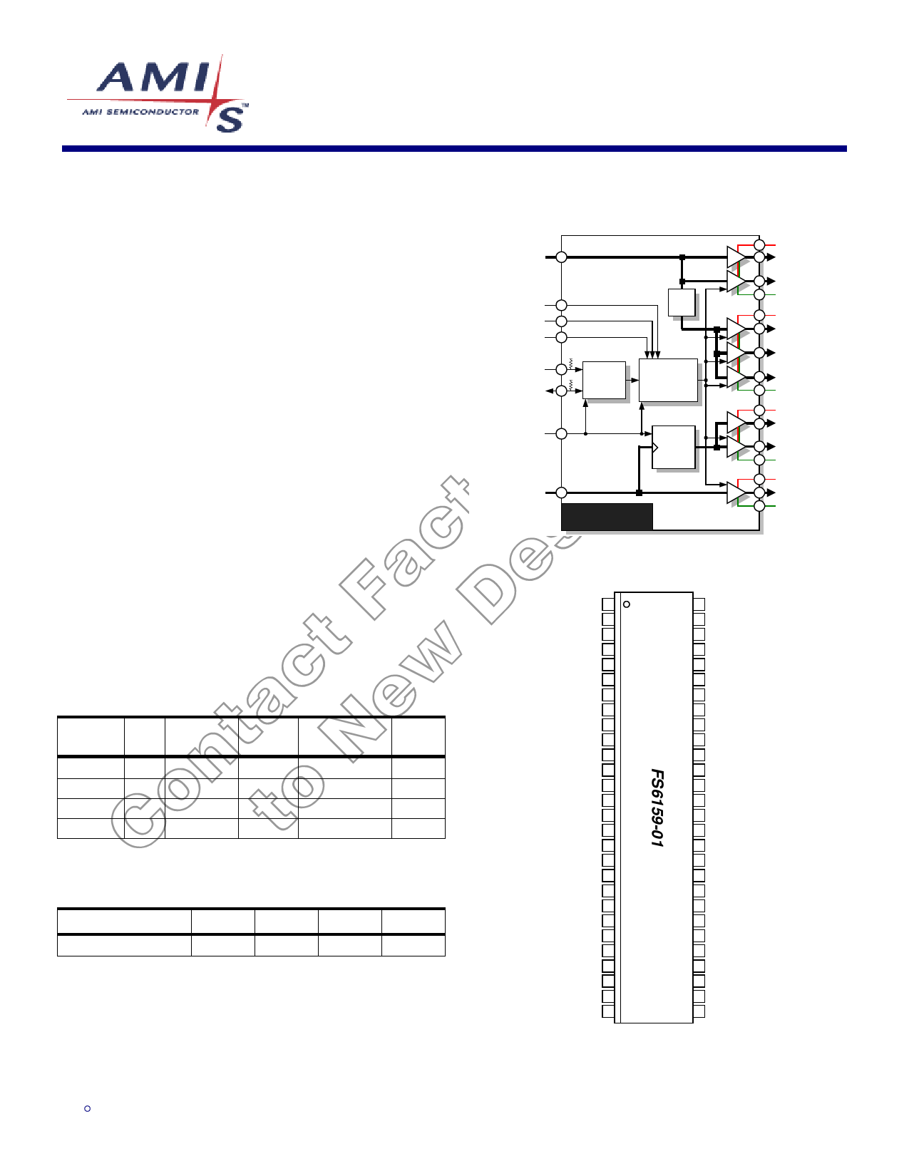
Figure 1: Block Diagram
66REF
SEL_Q
SEL_R
SEL_S
SCL
SDA
PWR_DWN#
÷2
SMBus
Output
Control
PLL
14REF
FS6159
Figure 2: Pin Configuration
VSS_N 1
14REF 2
VDD_N 3
66REF 4
VSS_P 5
PCI_0 6
PCI_1 7
VDD_P 8
VSS_P 9
PCI_2 10
PCI_3 11
VDD_P 12
VSS_P 13
PCI_4 14
PCI_5 15
VDD_P 16
PCI_6 17
PCI_7 18
VSS_P 19
VDD_P 20
PCI_8 21
PCI_9 22
VSS_P 23
PCI_10 24
PCI_11 25
VDD_P 26
SEL_Q 27
SEL_R 28
56 VDD_R
55 REF_1
54 REF_0
53 VSS_R
52 VDD_66
51 CK66_5
50 CK66_4
49 VSS_66
48 VSS_66
47 CK66_3
46 CK66_2
45 VDD_66
44 VDD_66
43 CK66_1
42 CK66_0
41 VSS_66
40 VDD
39 VSS
38 VDD_48
37 CK48_1
36 CK48_0
35 VSS_48
34 SEL_S
33 PWR_DWN#
32 VDD_S
31 VSS_S
30 SCL
29 SDA
VDD_66
CK66_0:4
CK66_5
VSS_66
VDD_P
PCI_0:5
PCI_6:7
PCI_8:11
VSS_P
VDD_48
CK48_0
CK48_1
VSS_48
VDD_R
REF_0:1
VSS_R
Intel and Pentium are registered trademarks of Intel Corporation. Lexmark is a trademark of Lexmark International, Inc. Non-linear spread spectrum modulation profile is licensed under US Patent
No. 5488627, Lexmark International, Inc. This document contains information on a preproduction product. Specifications and information herein are subject to change without notice.
ISO9001
2.27.02
IntFF
Share Link: 