MC33975ATEKR2 데이터 시트보기 (PDF) - Freescale Semiconductor
부품명
상세내역
제조사
MC33975ATEKR2
Freescale Semiconductor

MC33975ATEKR2 Datasheet PDF : 32 Pages
| |||
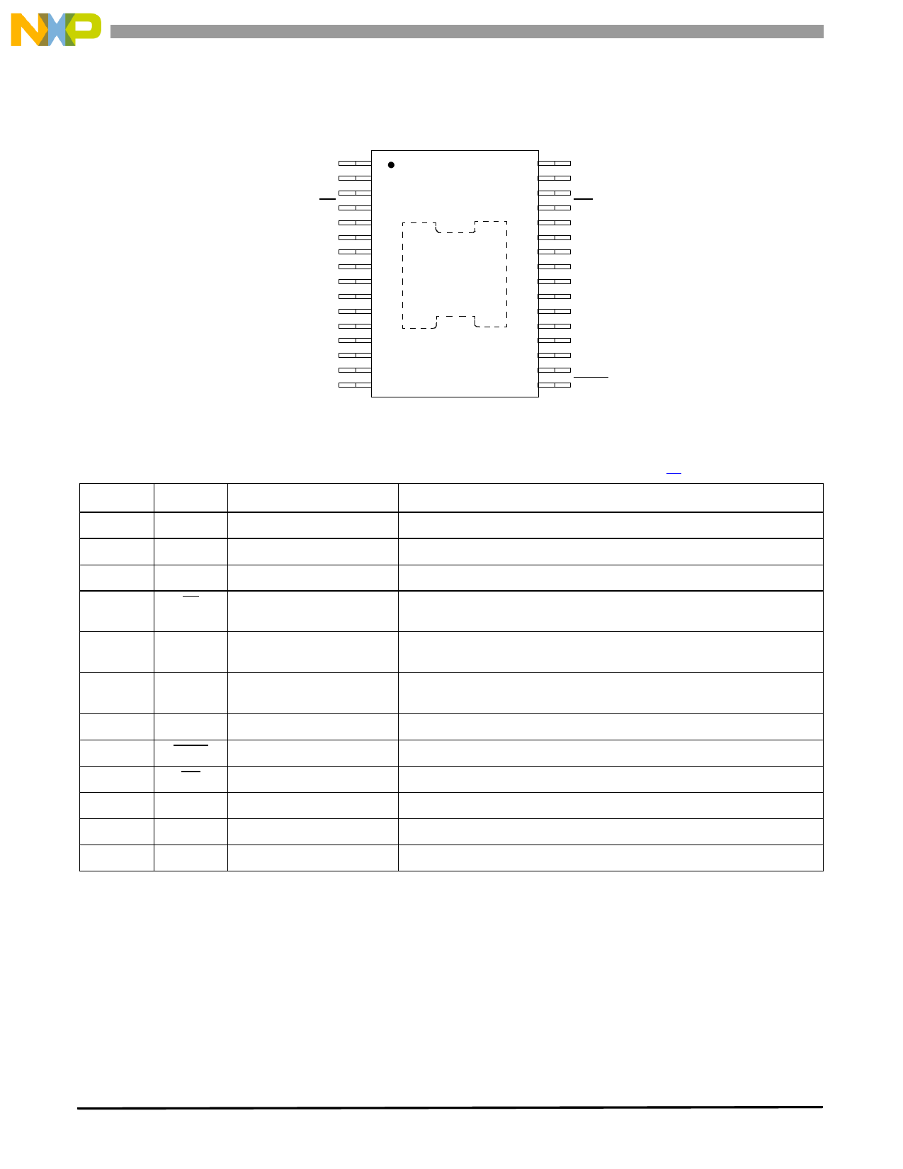
PIN CONNECTIONS
PIN CONNECTIONS
GND
1
SI
2
SCLK
3
CS
4
SP0
5
SP1
6
SP2
7
SP3
8
SG0
9
SG1
10
SG2
11
SG3
12
SG4
13
SG5
14
SG6
15
VPWR
16
32
SO
31
VDD
30
AMUX
29
INT
28
SP7
27
SP6
26
SP5
25
SP4
24
SG7
23
SG8
22
SG9
21
SG10
20
SG11
19
SG12
18
SG13
17
WAKE
Figure 3. 33975 Pin Connections
Table 2. Pin Definitions
A functional description of each Pin can be found in the Functional Pin Description section on page 12.
Pin
Pin Name
Formal Name
Description
1
GND
2
SI
3
SCLK
4
CS
Ground
SPI Slave In
Serial Clock
Chip Select
Ground for logic, analog, and switch-to-battery inputs
SPI control data input pin from MCU to 33975
SPI control clock input pin
SPI control chip select input pin from MCU to 33975. Logic [0] allows data to be
transferred in
5–8
25 – 28
9 – 15,
18 – 24
16
17
29
30
31
32
SPn
SGn
VPWR
WAKE
INT
AMUX
VDD
SO
Programmable Switches 0–3
Programmable Switches 4–7
Switch-to-Ground Inputs 0–6
Switch-to-Ground Inputs 13–7
Battery Input
Wake-up
Interrupt
Analog Multiplex Output
Voltage Drain Supply
SPI Slave Out
Programmable switch-to-battery or switch-to-ground input pins
Switch-to-ground input pins
Battery supply input pin. This pin requires external reverse battery protection.
Open drain wake-up output is designed to control a power supply enable pin
Open-drain output to MCU is used to indicate input switch change of state
Analog multiplex output
3.3/5.0 V supply sets SPI communication level for the SO driver
Provides digital data from 33975 to the MCU
33975
4
Analog Integrated Circuit Device Data
Freescale Semiconductor
Share Link: