33981B 데이터 시트보기 (PDF) - Freescale Semiconductor
부품명
상세내역
제조사
33981B Datasheet PDF : 37 Pages
| |||
ELECTRICAL CHARACTERISTICS
MAXIMUM RATINGS
ELECTRICAL CHARACTERISTICS
MAXIMUM RATINGS
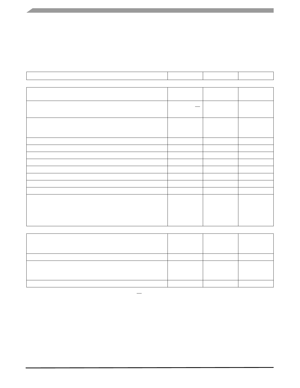
Table 2. Maximum Ratings
All voltages are with respect to ground unless otherwise noted.
Rating
Symbol
Value
Unit
ELECTRICAL RATINGS
Power Supply Voltage
Steady-state
Input/Output Pins Voltage(1)
Output Voltage
Positive
Negative
Continuous Output Current(2)
CSNS Input Clamp Current
EN Input Clamp Current
SR Voltage
CBOOT Voltage
OCLS Voltage
Low Side Gate Voltage
Low Side Drain Voltage
ESD Voltage(3)
Human Body Model (HBM)
Charge Device Model (CDM)
Corner Pins (1, 12, 15, 16)
All Other Pins (2-11, 13-14)
VPWR
V
-16 to 41
INHS, INLS,
- 0.3 to 7.0
V
CONF, CSNS, FS,
TEMP, EN
VOUT
V
41.0
-5.0
IOUT
40.0
A
ICL(CSNS)
15.0
mA
ICL(EN)
2.5
mA
VSR
- 0.3 to 54.0
V
CBOOT
- 0.3 to 54.0
V
VOCLS
- 5.0 to 7.0
V
VGLS
- 0.3 to 15.0
V
VDLS
- 5.0 to 41.0
V
VESD
V
± 2000
± 750
± 500
THERMAL RATINGS
Operating Temperature
Ambient
Junction
°C
TA
- 40 to 125
TJ
- 40 to 150
Storage Temperature
Thermal Resistance(4)
Junction to Power Die Case
Junction to Ambient
Peak Package Reflow Temperature During Reflow(5), (6)
TSTG
RθJC
RθJA
TPPRT
- 55 to 150
1.0
30.0
Note 6
°C
°C/W
°C
Notes
1. Exceeding voltage limits on INHS, INLS, CONF, CSNS, FS, TEMP, and EN pins may cause a malfunction or permanent damage to the
device.
2. Continuous high side output rating as long as maximum junction temperature is not exceeded. Calculation of maximum output current
using package thermal resistance is required.
3. ESD testing is performed in accordance with the Human Body Model (HBM) (CZAP = 100 pF, RZAP = 1500 Ω) and the Charge Device
Model (CDM), Robotic (CZAP = 4.0 pF).
4. Device mounted on a 2s2p test board per JEDEC JESD51-2.
5. Pin soldering temperature limit is for 10 seconds maximum duration. Not designed for immersion soldering. Exceeding these limits may
cause malfunction or permanent damage to the device.
6. Freescale’s Package Reflow capability meets Pb-free requirements for JEDEC standard J-STD-020C. For Peak Package Reflow
Temperature and Moisture Sensitivity Levels (MSL), Go to www.freescale.com, search by part number [e.g. remove prefixes/suffixes
and enter the core ID to view all orderable parts. (i.e. MC33xxxD enter 33xxx), and review parametrics.
33981
4
Analog Integrated Circuit Device Data
Freescale Semiconductor
Share Link: 