ADP3203 데이터 시트보기 (PDF) - Analog Devices
부품명
상세내역
제조사
ADP3203 Datasheet PDF : 16 Pages
| |||
a
2-Phase IMVP-II and IMVP-III
Core Controller for Mobile CPUs
ADP3203
FEATURES
Pin Selectable 1- or 2-Phase Operation
Static and Dynamic Current Sharing Characteristics
Backward Compatible to IMVP-II
Superior Load Transient Response with ADOPTTM
Optimal Positioning Technology
Noise Blanking for Speed and Stability
Synchronous Rectifier Control Extends Battery Life
Smooth Output Transition During VID Code Change
Cycle-by-Cycle Current Limiting
Hiccup or Latched Overload Protection
Transient Glitch-Free Power Good
Soft Start Eliminates Power-On In-Rush Current Surge
2-Level Overvoltage and Reverse Voltage Protection
APPLICATIONS
IMVP-II and IMVP-III Core DC-to-DC Converters
Fixed Voltage Mobile CPU Core DC-to-DC Converters
Notebook/Laptop Power Supplies
Programmable Output Power Supplies
GENERAL DESCRIPTION
The ADP3203 is a 1- or 2-phase hysteretic peak current dc-to-dc
buck converter controller dedicated to power a mobile
processor’s core. The optimized low voltage design is powered
from the 3.3 V system supply and draws only 10 µA maximum
in shutdown. The nominal output voltage is set by a 5-bit VID
code. To accommodate the transition time required by the
newest processors for on-the-fly VID changes, the ADP3203
features high speed operation to allow a minimized inductor size
that results in the fastest change of current to the output. To
further allow for the minimum number of output capacitors to
be used, the ADP3203 features active voltage positioning with
ADOPT optimal compensation to ensure a superior load transient
response. The output signal interfaces with the ADP3415
MOSFET driver that is optimized for high speed and high effi-
ciency for driving both the top and bottom MOSFETs of the buck
converter. The ADP3203 is capable of controlling the synchronous
rectifier to extend battery lifetime in light load conditions.
HYSSET
DSHIFT
BSHIFT
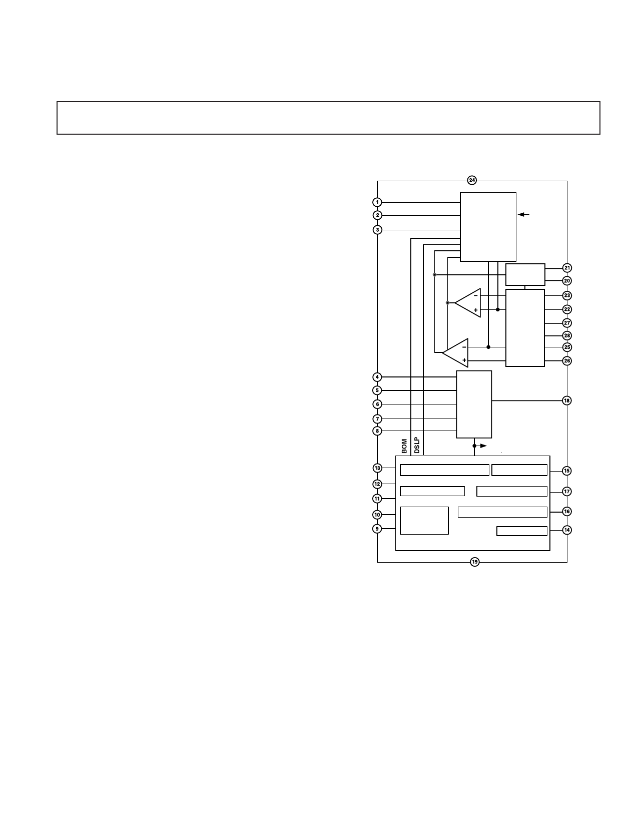
FUNCTIONAL BLOCK DIAGRAM
VCC
ADP3203
HYSTERESIS
VR
SETTING
AND
SHIFT-MUX
VID4
VID3
VID2
VID1
VID0
SD
PWRGD
DPRSLP
DSLP
BOM
CLIM
EN
CORE
PHASE
SPLITTER
CURRENT
SENSE
MUX
5-BIT VID
DAC
AND
FIXED
REF
VR
ENABLE _UVLO MAIN BIAS SR CONTROL
PWRGD BLANKER
COREGD MONITOR
VID MUX AND
SHIFT
SELECTOR
SS-HICCUP TIMER AND OCP
OVP AND RVP
PM MODULE
GND
OUT2
OUT1
CS2
CS1
CS+
CS–
RAMP
REG
DACOUT
DRVLSD
COREFB
SS
CLAMP
ADOPT is a trademark of Analog Devices.
REV. 0
Information furnished by Analog Devices is believed to be accurate and
reliable. However, no responsibility is assumed by Analog Devices for its
use, nor for any infringements of patents or other rights of third parties that
may result from its use. No license is granted by implication or otherwise
under any patent or patent rights of Analog Devices.
One Technology Way, P.O. Box 9106, Norwood, MA 02062-9106, U.S.A.
Tel: 781/329-4700
www.analog.com
Fax: 781/326-8703
© Analog Devices, Inc., 2002
Share Link: 