AWC6312RM9Q7 데이터 시트보기 (PDF) - ANADIGICS
부품명
상세내역
제조사
AWC6312RM9Q7 Datasheet PDF : 8 Pages
| |||
ELECTRICAL CHARACTERISTICS
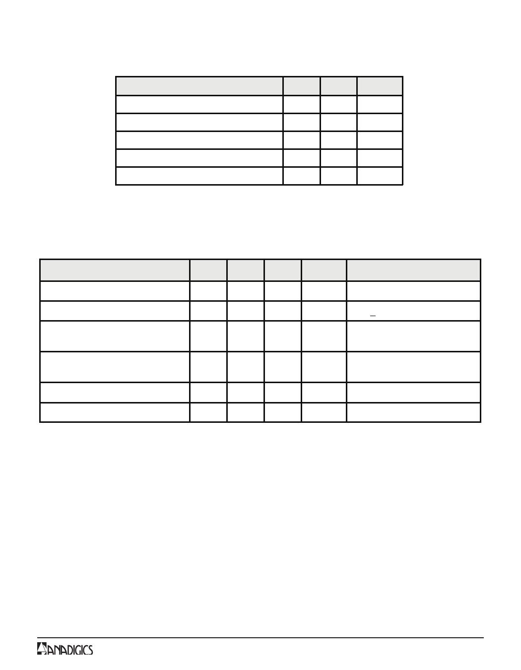
Table 2: Absolute Minimum and Maximum Ratings
PARAMETER
MIN MAX UNIT
Supply Voltage (VCC and VBATT)
0
+5
V
Mode Control Voltage (VMODE)
0
+3.5
V
Enable Voltage (VEN)
0
+3.5
V
RF Input Power (PIN)
-
+10
dBm
Storage Temperature (TSTG)
-40 +150
°C
Stresses in excess of the absolute ratings may cause permanent damage.
Functional operation is not implied under these conditions. Exposure
to absolute ratings for extended periods of time may adversely affect
reliability.
AWC6312R
PARAMETER
Table 3: Operating Ranges
MIN TYP MAX UNIT
COMMENTS
Operating Frequency (f)
1850
-
1915 MHz
Supply Voltage (VCC and VBATT)
+3.2 +3.4 +4.2
V
POUT < 28.0 dBm
Enable Voltage (VEN)
+2.2 +2.4 +3.1
0
-
+0.5
V
PA "on"
PA "shut down"
Mode Control Voltage (VMODE)
+2.2 +2.4 +3.1
0
-
+0.5
V
Low Bias Mode
High Bias Mode
RF Output Power (POUT)
27.5 (1) +28.0
-
dBm
Case Temperature (TC)
-30
-
+85
°C
The device may be operated safely over these conditions; however, parametric performance is guaranteed only
over the conditions defined in the electrical specifications.
Notes:
(1) For operation at Vcc = +3.2 V, Pout is derated by 0.5 dB.
Data Sheet - Rev 2.0
3
01/2009
Share Link: 