SPX5205M5-4.0 데이터 시트보기 (PDF) - Signal Processing Technologies
부품명
상세내역
제조사
SPX5205M5-4.0 Datasheet PDF : 9 Pages
| |||
Application Hints
The SPX5205 requires an output capacitor for device stability.
The value required varies greatly depending upon the
application circuit. The high frequency characteristics of
electrolytic capacitors depend greatly on the type and also on
the manufacturer. Sometimes bench testing is the only means
to determine the proper capacitor type and value. The high
quality 2.2µF aluminum electrolytic capacitor covers all
general application circuits; this stability can be obtained with
a tantalum electrolytic value of 1µF.
SPX5205
In general, linear regulator stability decreases with higher
output currents. In most applications the SPX5205 is
operating at few milliamps. In these applications the output
capacitance can be further reduced. For example, when the
regulator is running at 10mA output current the output
capacitance value is half compared to the same regulator
that is running at 150mA.
With the SPX5205 adjustable regulator, the minimum value
of output capacitance is a function of the output voltage.
The value decreases with higher output voltages, since the
closed loop gain is increased.
Typical Applications Circuits
The SPX5205 provides access to the internal reference. A 10µF capacitor on the BYP pin will provide a significant reduction in
output noise. This pin may be left unconnected if the output noise is not a major concern. The SPX5205 start-up speed is inversely
proportional to the size of this capacitor. Applications requiring a slow ramp-up of output voltage should consider larger values of
CBYP. If the rapid turn-ON is necessary, omit bypass capacitor.
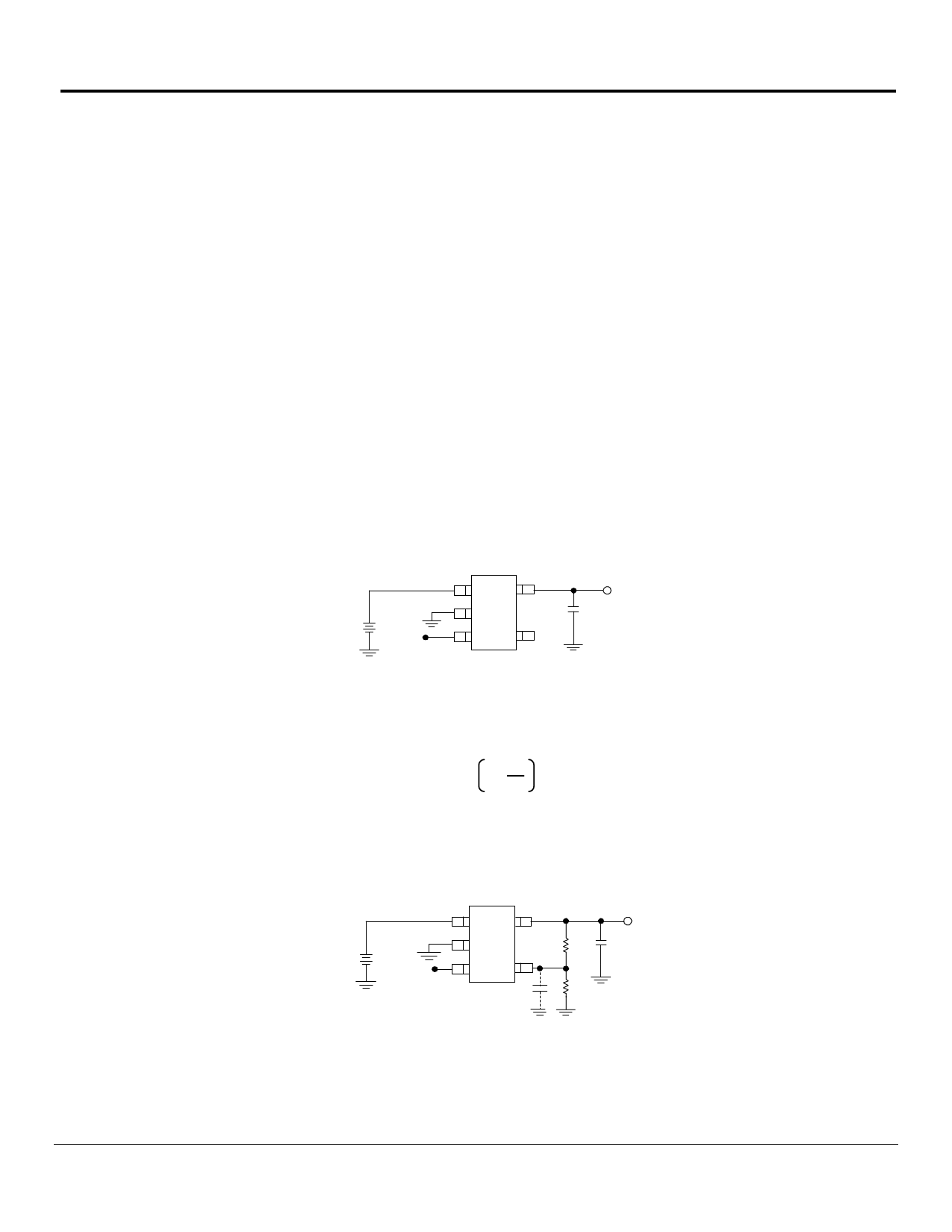
Figure 1 shows SPX5205 standard application circuit. The EN pin is pulled high (>2.0V) to enable the regulator. To disable the
regulator, EN < 0.6V.
VIN
1
5
VOUT
+ GND
EN
2
+
SPX5205
3
4 BYP
(Optn)
Hi-ON
Lo-OFF
Top View
Fig. 1
The SPX5205 in figure 2 shows adjustable output voltage configuration. Two resistors set the output voltage. The formula for output
voltage is:
VOUT = 1.235 x
1+
R1
R2
Resistor values are not critical as the ADJ pin has high input impedance, for best results use resistors of 47kΩ or less. A capacitor
from ADJ to ground will provide improved noise performance.
VIN
+ GND
EN
Hi-ON
Lo-OFF
1
5
VOUT
2
+
3 SPX5205 4 ADJ R1
Byp
R2
(Optn)
Top View
Fig. 2
Rev. 10/24/00
Share Link: 