CY7C128A-15VC 데이터 시트보기 (PDF) - Cypress Semiconductor
부품명
상세내역
제조사
CY7C128A-15VC Datasheet PDF : 10 Pages
| |||
CY7C128A
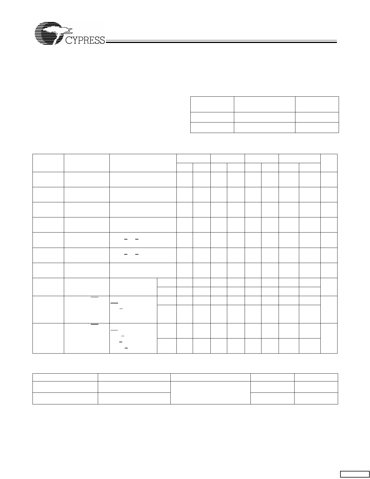
Maximum Ratings
(Above which the useful life may be impaired. For user guide-
lines, not tested.)
Storage Temperature ................................. –65°C to +150°C
Ambient Temperature with
Power Applied............................................. –55°C to +125°C
Supply Voltage to Ground Potential
(Pin 28 to Pin 14) ........................................... –0.5V to +7.0V
DC Voltage Applied to Outputs
in High Z State ............................................... –0.5V to +7.0V
DC Input Voltage............................................ –3.0V to +7.0V
Output Current into Outputs (LOW)............................. 20 mA
Static Discharge Voltage .......................................... >2001V
(per MIL-STD-883, Method 3015)
Latch-Up Current.................................................... >200 mA
Operating Range
Range
Commercial
Military[1]
Ambient
Temperature
0°C to +70°C
–55°C to +125°C
VCC
5V ± 10%
5V ± 10%
Electrical Characteristics Over the Operating Range[2]
Parameter Description
VOH
Output HIGH
Voltage
VOL
Output LOW
Voltage
VIH
Input HIGH
Voltage
VIL
Input LOW
Voltage[3]
IIX
Input Load
Current
IOZ
Output Leakage
Current
IOS
Output Short
Circuit Current[4]
ICC
VCC Operating
Supply Current
ISB1
Automatic CE
Power-Down
Current
ISB2
Automatic CE
Power-Down
Current
Test Conditions
VCC = Min.,
IOH = –4.0 mA
VCC = Min., IOL = 8.0 mA
GND < VI < VCC
GND < VI < VCC
Output Disabled
VCC = Max.,
VOUT = GND
VCC = Max.
IOUT = 0 mA
Max. VCC,
CE > VIH,
Min. Duty Cycle
= 100%
Max. VCC,
CE1 >VCC–0.3V,
VIN > VCC–0.3V
or VIN < 0.3V
Com’l
Mil
Com’l
Mil
Com’l
Mil
7C128A-15 7C128A-20 7C128A-25 7C128A-35,45
Min. Max. Min. Max. Min. Max. Min. Max. Unit
2.4
2.4
2.4
2.4
V
0.4
0.4
0.4
0.4 V
2.2 VCC 2.2 VCC 2.2 VCC 2.2
VCC
V
–0.5 0.8 –0.5 0.8 –0.5 0.8 –0.5 0.8 V
–10 +10 –10 +10 –10 +10 –10 +10 µA
–10 +10 –10 +10 –10 +10 –10 +10 µA
–300
–300
–300
–300 mA
120
120
120
-
125
125
40
40
20
-
40
40
120 mA
125
20 mA
20
40
20
20
-
20
20
20 mA
20
Capacitance[5]
Parameter
CIN
COUT
Description
Input Capacitance
Output Capacitance
Test Conditions
TA = 25°C, f = 1 MHz,
VCC = 5.0V
Notes:
1. TA is the “instant on” case temperature.
2. See the last page of this specification for Group A subgroup testing information.
3. VIL (min.) = –3.0V for pulse durations less than 30 ns.
4. Not more than 1 output should be shorted at one time. Duration of the short circuit should not exceed 30 seconds.
5. Tested initially and after any design or process changes that may affect these parameters.
Max.
10
10
Unit
pF
pF
Document #: 38-05028 Rev. **
Page 2 of 10
[+] Feedback
Share Link: 