28F160S3-140 데이터 시트보기 (PDF) - Intel
부품명
상세내역
제조사
28F160S3-140 Datasheet PDF : 52 Pages
| |||
28F160S3, 28F320S3
E
The device incorporates two Write Buffers of 32
bytes (16 words) to allow optimum-performance
data programming. This feature can improve
system program performance by up to four times
over non-buffer programming.
Individual block locking uses a combination of block
lock-bits to lock and unlock blocks. Block lock-bits
gate block erase, full chip erase, program and write
to buffer operations. Lock-bit configuration
operations (Set Block Lock-Bit and Clear Block
Lock-Bits commands) set and clear lock-bits.
The Status Register and the STS pin in RY/BY#
mode indicate whether or not the device is busy
executing an operation or ready for a new
command. Polling the Status Register, system
software retrieves WSM feedback. STS in RY/BY#
mode gives an additional indicator of WSM activity
by providing a hardware status signal. Like the
Status Register, RY/BY#-low indicates that the
WSM is performing a block erase, program, or lock-
bit operation. RY/BY#-high indicates that the WSM
is ready for a new command, block erase is
suspended (and program is inactive), program is
suspended, or the device is in deep power-down
mode.
The Automatic Power Savings (APS) feature
substantially reduces active current when the
device is in static mode (addresses not switching).
The BYTE# pin allows either x8 or x16 read/writes
to the device. BYTE# at logic low selects 8-bit
mode with address A0 selecting between the low
byte and high byte. BYTE# at logic high enables
16-bit operation with address A1 becoming the
lowest order address. Address A0 is not used in 16-
bit mode.
When one of the CEX# pins (CE0#, CE1#) and RP#
pins are at VCC, the component enters a CMOS
standby mode. Driving RP# to GND enables a deep
power-down mode which significantly reduces
power consumption, provides write protection,
resets the device, and clears the Status Register. A
reset time (tPHQV) is required from RP# switching
high until outputs are valid. Likewise, the device
has a wake time (tPHEL) from RP#-high until writes
to the CUI are recognized.
1.3 Pinout and Pin Description
The 16-Mbit device is available in the 56-lead
TSOP, 56-lead SSOP and µBGA packages. The
32- Mb device is available in the 56-lead SSOP and
µBGA packages. The pinouts are shown in Figures
2, 3 and 4.
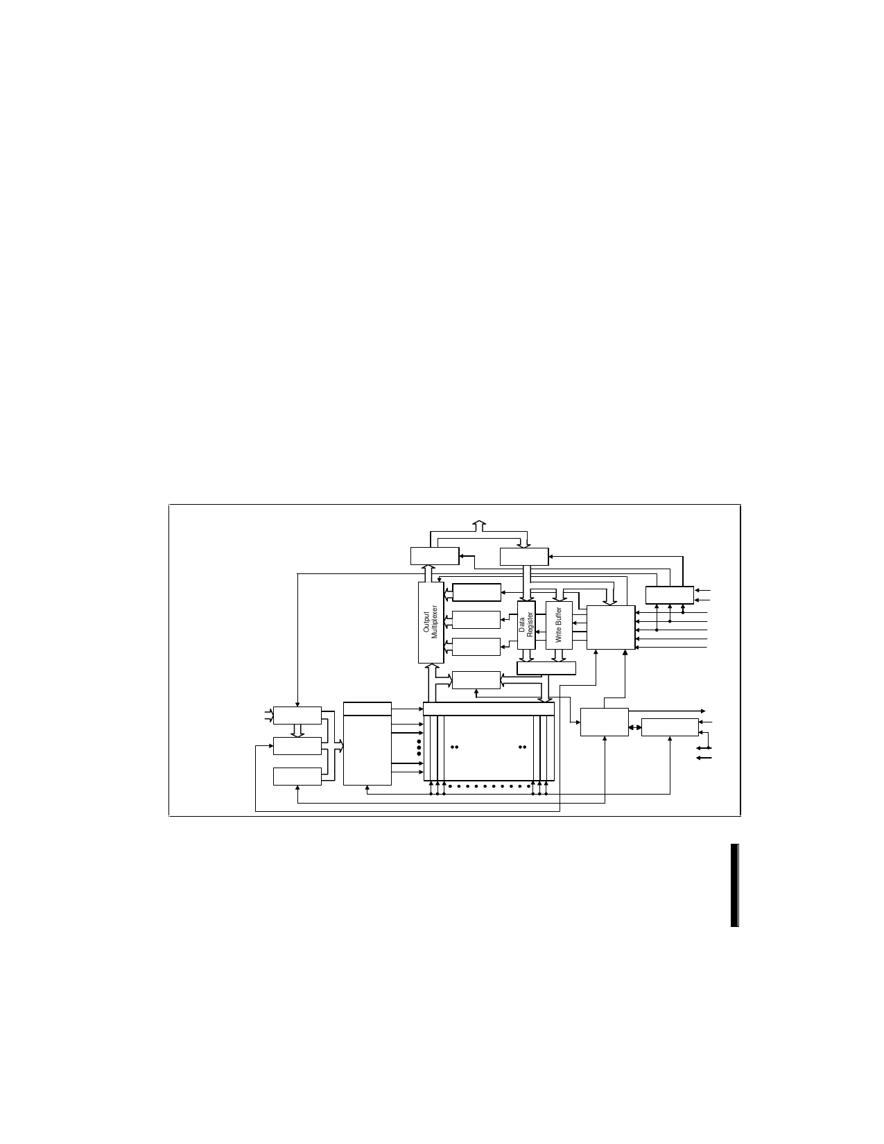
DQ0 - DQ15
16-Mbit: A0- A20
32-Mbit: A0 - A21
Input Buffer
Address
Latch
Address
Counter
Y-Decoder
X-Decoder
Output Buffer
Input Buffer
Query
Identifier
Register
Status
Register
Data
Comparator
Y-Gating
Multiplexer
16-Mbit: Thirty-two
32-Mbit: Sixty-four
64-Kbyte Blocks
Command
User
Interface
I/O Logic
VCC
BYTE#
CE#
WE#
OE#
RP#
WP#
Write State
Machine
Program/Erase
Voltage Switch
STS
VPP
VCC
GND
Figure 1. Block Diagram
6
ADVANCE INFORMATION
Share Link: 