EM658160 데이터 시트보기 (PDF) - Etron Technology
부품명
상세내역
제조사
EM658160 Datasheet PDF : 26 Pages
| |||
Et r onT ec h
4Mx16 DDR SDRAM
EM658160
Pin Descriptions
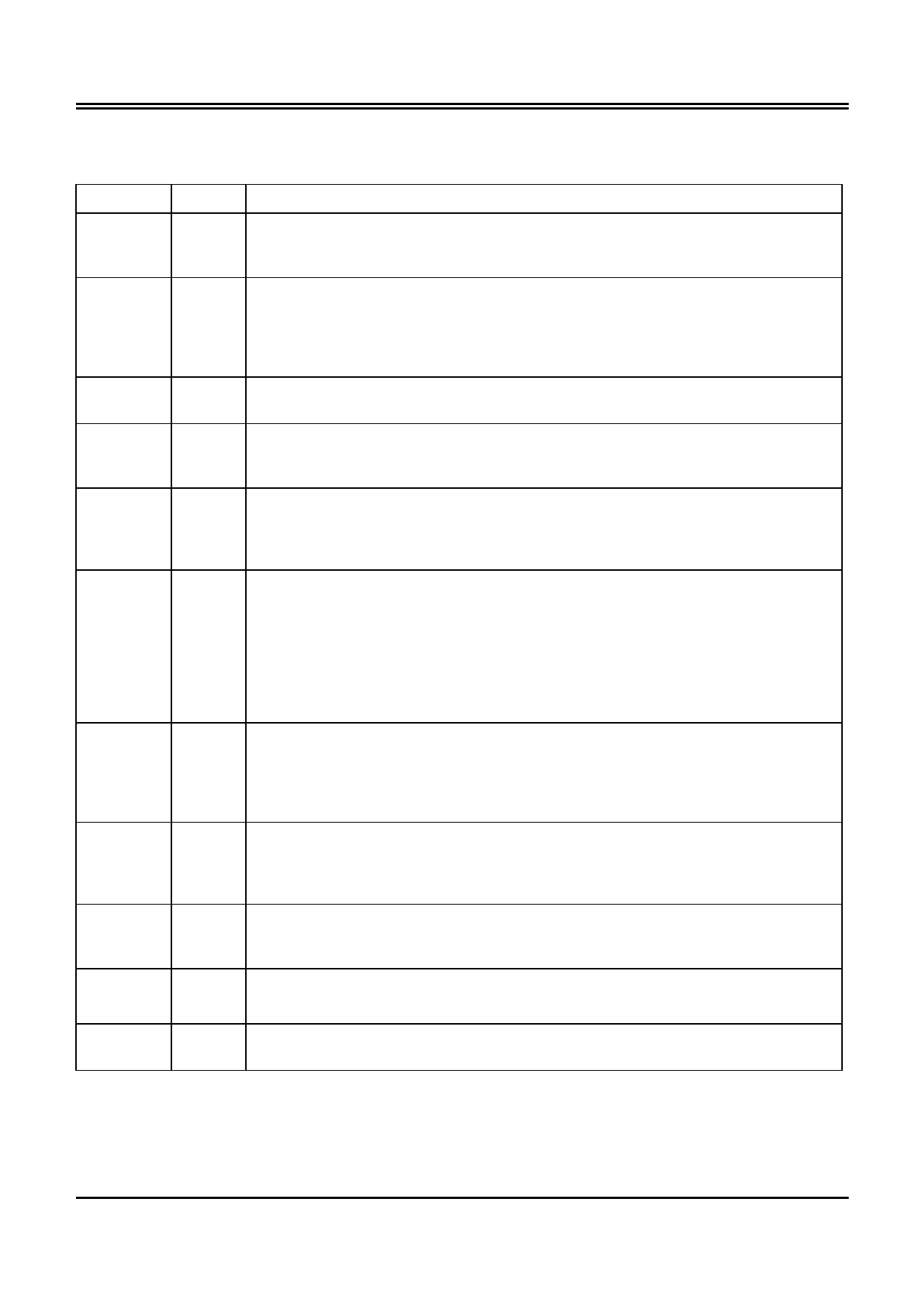
Table 1. Pin Details of EM658160
Symbol Type
Description
CK, /CK
Input
Differential Clock: CK, /CK are driven by the system clock. All SDRAM input signals
are sampled on the positive edge of CK. Both CK and /CK increment the internal burst
counter and controls the output registers.
CKE
Input
Clock Enable: CKE activates(HIGH) and deactivates(LOW) the CK signal. If CKE
goes low synchronously with clock, the internal clock is suspended from the next clock
cycle and the state of output and burst address is frozen as long as the CKE remains
low. When all banks are in the idle state, deactivating the clock controls the entry to
the Power Down and Self Refresh modes.
BS0, BS1
Input Bank Select: BS0 and BS1 defines to which bank the BankActivate, Read, Write, or
BankPrecharge command is being applied.
A0-A11
Input
Address Inputs: A0-A11 are sampled during the BankActivate command (row
address A0-A11) and Read/Write command (column address A0-A7with A10 defining
Auto Precharge).
/CS
Input Chip Select: /CS enables (sampled LOW) and disables (sampled HIGH) the
command decoder. All commands are masked when /CS is sampled HIGH. /CS
provides for external bank selection on systems with multiple banks. It is considered
part of the command code.
/RAS
Input
Row Address Strobe: The /RAS signal defines the operation commands in
conjunction with the /CAS and /WE signals and is latched at the positive edges of CK.
When /RAS and /CS are asserted "LOW" and /CAS is asserted "HIGH," either the
BankActivate command or the Precharge command is selected by the /WE signal.
When the /WE is asserted "HIGH," the BankActivate command is selected and the
bank designated by BS is turned on to the active state. When the /WE is asserted
"LOW," the Precharge command is selected and the bank designated by BS is
switched to the idle state after the precharge operation.
/CAS
Input
Column Address Strobe: The /CAS signal defines the operation commands in
conjunction with the /RAS and /WE signals and is latched at the positive edges of CK.
When /RAS is held "HIGH" and /CS is asserted "LOW," the column access is started
by asserting /CAS "LOW." Then, the Read or Write command is selected by asserting
/WE "HIGH " or LOW"."
/WE
Input Write Enable: The /WE signal defines the operation commands in conjunction with
the /RAS and /CAS signals and is latched at the positive edges of CK. The /WE input
is used to select the BankActivate or Precharge command and Read or Write
command.
LDQS,
UDQS
Input / Bidirectional Data Strobe: Specifies timing for Input and Output data. Read Data
Output
Strobe is edge triggered. Write Data Strobe provides a setup and hold time for data
and DQM. LDQS is for DQ0~7, UDQS is for DQ8~15.
LDM,
UDM
Input Data Input Mask: Input data is masked when DM is sampled HIGH during a write
cycle. LDM masks DQ0-DQ7, UDM masks DQ8-DQ15.
DQ0 - DQ15 Input / Data I/O: The DQ0-DQ15 input and output data are synchronized with the positive
Output edges of CK and /CK. The I/Os are byte-maskable during Writes.
Etron Confidential
3
Rev. 1.1
Jan. 2002
Share Link: 