FDG6331L 데이터 시트보기 (PDF) - Fairchild Semiconductor
부품명
상세내역
제조사
FDG6331L Datasheet PDF : 4 Pages
| |||
Electrical Characteristics
Symbol
Parameter
TA = 25°C unless otherwise noted
Test Conditions
Min Typ Max Units
Off Characteristics
BVIN
Vin Breakdown Voltage
VON/OFF = 0 V, ID = –250 µA
8
ILoad
Zero Gate Voltage Drain Current
VIN = –6.4 V, VON/OFF = 0 V
IFL
Leakage Current, Forward
VON/OFF = 0 V, VIN = 8 V
IRL
Leakage Current, Reverse
VON/OFF = 0 V, VIN = –8 V
On Characteristics (Note 2)
VON/OFF (th) Gate Threshold Voltage
RDS(on)
Static Drain–Source
On–Resistance (Q2)
RDS(on)
Static Drain–Source
On–Resistance (Q1)
VIN = VON/OFF, ID = –250 µA
0.4
VIN = 4.5 V,
VIN =2.5 V,
VIN = 1.8 V,
ID = –0.8 A
ID = –0.7 A
ID = –0.6 A
VIN = 4.5 V,
VIN = 2.7 V,
ID = 0.4A
ID = 0.2 A
Drain–Source Diode Characteristics and Maximum Ratings
IS
Maximum Continuous Drain–Source Diode Forward Current
VSD
Drain–Source Diode Forward
Voltage
VON/OFF = 0 V, IS = –0.25 A(Note 2)
V
–1
µA
100 nA
–100 nA
0.9
1.5
V
155
260 mΩ
193 330
248 450
310
400 mΩ
380 500
–0.25 A
–1.2
V
Notes:
1. RθJA is the sum of the junction-to-case and case-to-ambient thermal resistance where the case thermal reference is defined as the solder mounting surface of
the drain pins. RθJC is guaranteed by design while RθJA is determined by the user’s board design.
2. Pulse Test: Pulse Width < 300µs, Duty Cycle < 2.0%.
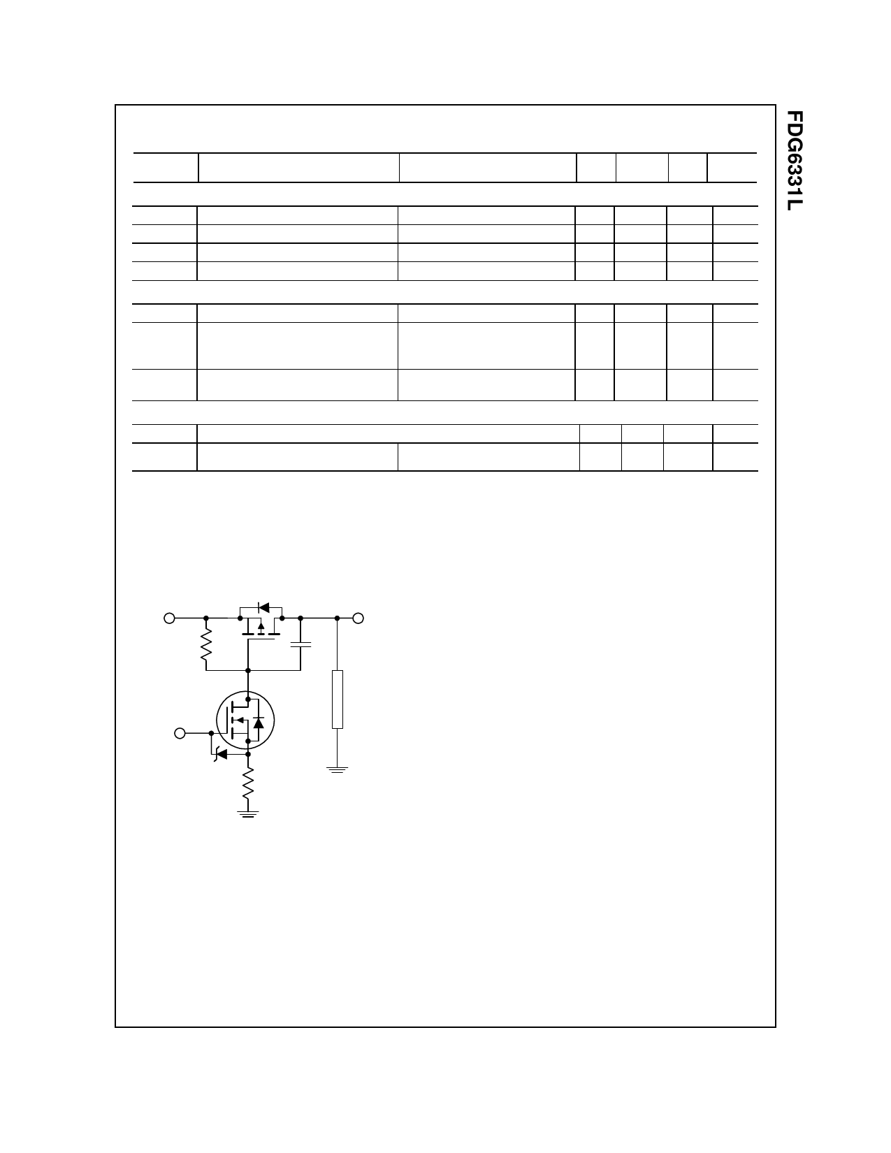
FDG6331L Load Switch Application Circuit
IN
Q2
OUT
C1
R1
Q1
ON/OFF
LOAD
R2
External Component Recommendation:
For additional in-rush current control, R2 and C1 can be added. For more information, see application note AN1030.
FDG6331L Rev B (W)
Share Link: 