IDT72413L35D 데이터 시트보기 (PDF) - Integrated Device Technology
부품명
상세내역
제조사
IDT72413L35D Datasheet PDF : 11 Pages
| |||
IDT72413
CMOS PARALLEL 64 x 5-BIT FIFO WITH FLAGS
MILITARY AND COMMERCIAL TEMPERATURE RANGES
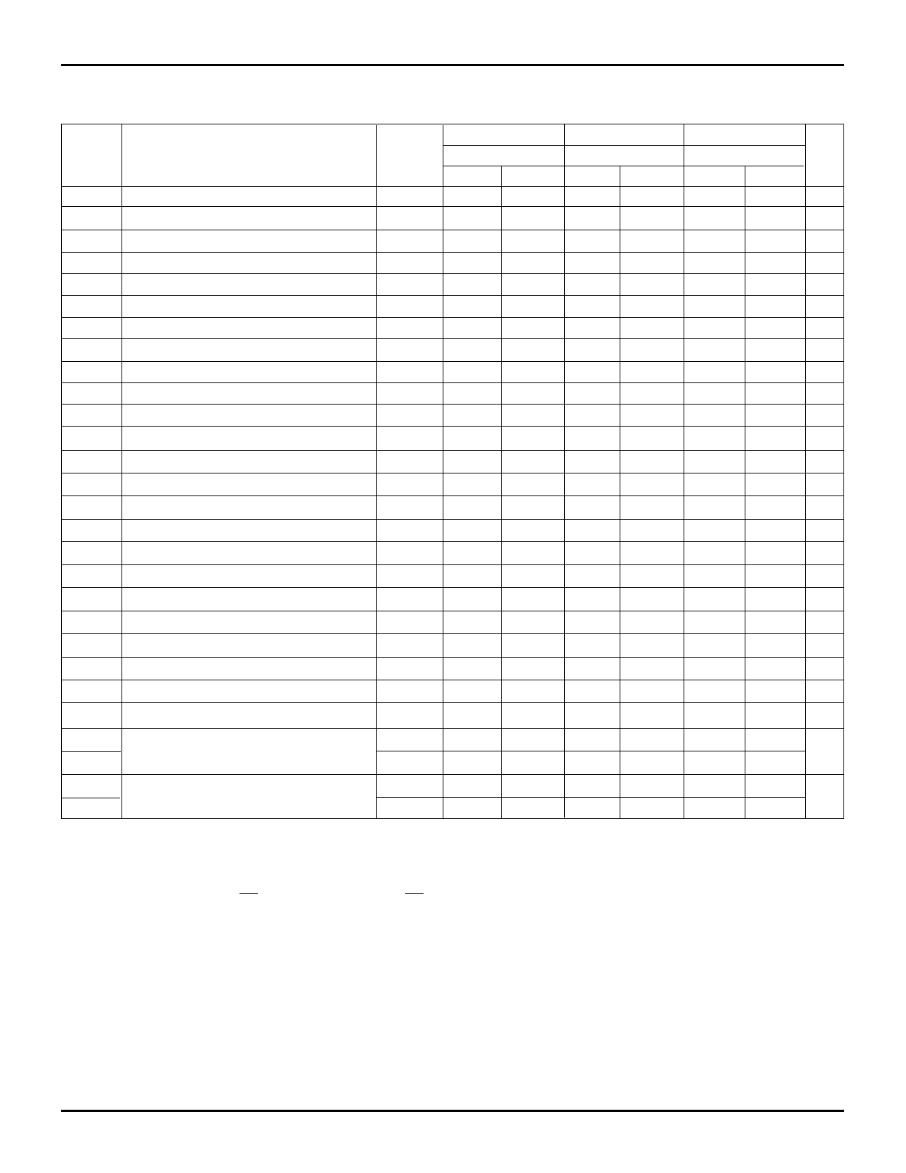
AC ELECTRICAL CHARACTERISTICS
(Commercial: VCC = 5.0V ± 10%, TA = 0°C to +70°C; Military: VCC = 5.0V ± 10%, TA = –55°C to +125°C)
Symbol
Parameters
Figure
Commercial
IDT72413L45
Min. Max.
Mil. & Com'l
IDT72413L35
Min. Max.
Mil. & Com'l
IDT72413L25
Min. Max. Unit
fIN
tIRL(1)
tIRH(1)
Shift In Rate
Shift In ↑ to Input Ready LOW
Shift In ↓ to Input Ready HIGH
2
—
45
—
35
—
25 MHz
2
—
18
—
18
—
28
ns
2
—
18
—
20
—
25
ns
fOUT
tORL(1)
tORH(1)
tODH(1)
Shift Out Rate
Shift Out ↓ to Output Ready LOW
Shift Out ↓ to Output Ready HIGH
Output Data Hold Previous Word
5
—
45
—
35
—
25 MHz
5
—
18
—
18
—
28
ns
5
—
19
—
20
—
25
ns
5
5
—
5
—
5
—
ns
tODS
Output Data Shift Next Word
5
—
19
—
20
—
20
ns
tPT
Data Throughput or "Fall-Through"
4, 7
—
25
—
28
—
40
ns
tMRORL Master Reset ↓ to Output Ready LOW
8
—
25
—
28
—
30
ns
tMRIRH(3) Master Reset ↑ to Input Ready HIGH
8
—
25
—
28
—
30
ns
tMRIRL(2) Master Reset ↓ to Input Ready LOW
8
—
25
—
28
—
30
ns
tMRQ
Master Reset ↓ to Outputs LOW
8
—
20
—
25
—
35
ns
tMRHF Master Reset ↓ to Half-Full Flag
8
—
25
—
28
—
40
ns
tMRAFE
tIPH(3)
tOPH(3)
t ORD(3)
Master Reset ↓ to AF/E Flag
Input Ready Pulse HIGH
Ouput Ready Pulse HIGH
Output Ready ↑ HIGH to Valid Data
8
—
25
—
28
—
40
ns
4
5
—
5
—
5
—
ns
7
5
—
5
—
5
—
ns
5
—
5
—
5
—
7
ns
tAEH
Shift Out ↑ to AF/E HIGH
9
—
28
—
28
—
40
ns
tAEL
Shift In ↑ to AF/E
9
—
28
—
28
—
40
ns
tAFL
Shift Out ↑ to AF/E LOW
10
—
28
—
28
—
40
ns
tAFH
Shift In ↑ to AF/E HIGH
10
—
28
—
28
—
40
ns
tHFH
Shift In ↑ to HF HIGH
11
—
28
—
28
—
40
ns
tHFL
tPHZ(3)
tPLZ(3)
tPLZ(3)
tPHZ(3)
Shif Out ↑ to HF LOW
Output Disable Delay
Output Enable Delay
11
—
28
—
28
—
40
ns
12
—
12
—
12
—
15
ns
12
—
12
—
12
—
15
12
—
15
—
15
—
20
ns
12
—
15
—
15
—
20
NOTES:
2748 tbl 06
1. Since the FIFO is a very high-speed device, care must be taken in the design of the hardware and the timing utilized within the design. Device grounding
and decoupling are crucial to correct operation as the FIFO will respond to very small glitches due to long reflective lines, high capacitances and/or poor
supply decoupling and grounding. A monolithic ceramic capacitor of 0.1µF directly between VCC and GND with very short lead length is recommended.
2. If the FIFO is full, (IR = HIGH), MR ↓ forces IR to go LOW, and MR ↑ causes IR to go HIGH.
3. Guaranteed by design but not currently tested.
5.02
4
Share Link: 