IDT54FCT162260AT 데이터 시트보기 (PDF) - Integrated Device Technology
부품명
상세내역
제조사
IDT54FCT162260AT Datasheet PDF : 8 Pages
| |||
IDT54/74FCT16260AT/CT/ET, 162260AT/CT/ET
FAST CMOS 12-BIT TRI-PORT BUS EXCHANGER
MILITARY AND COMMERCIAL TEMPERATURES RANGES
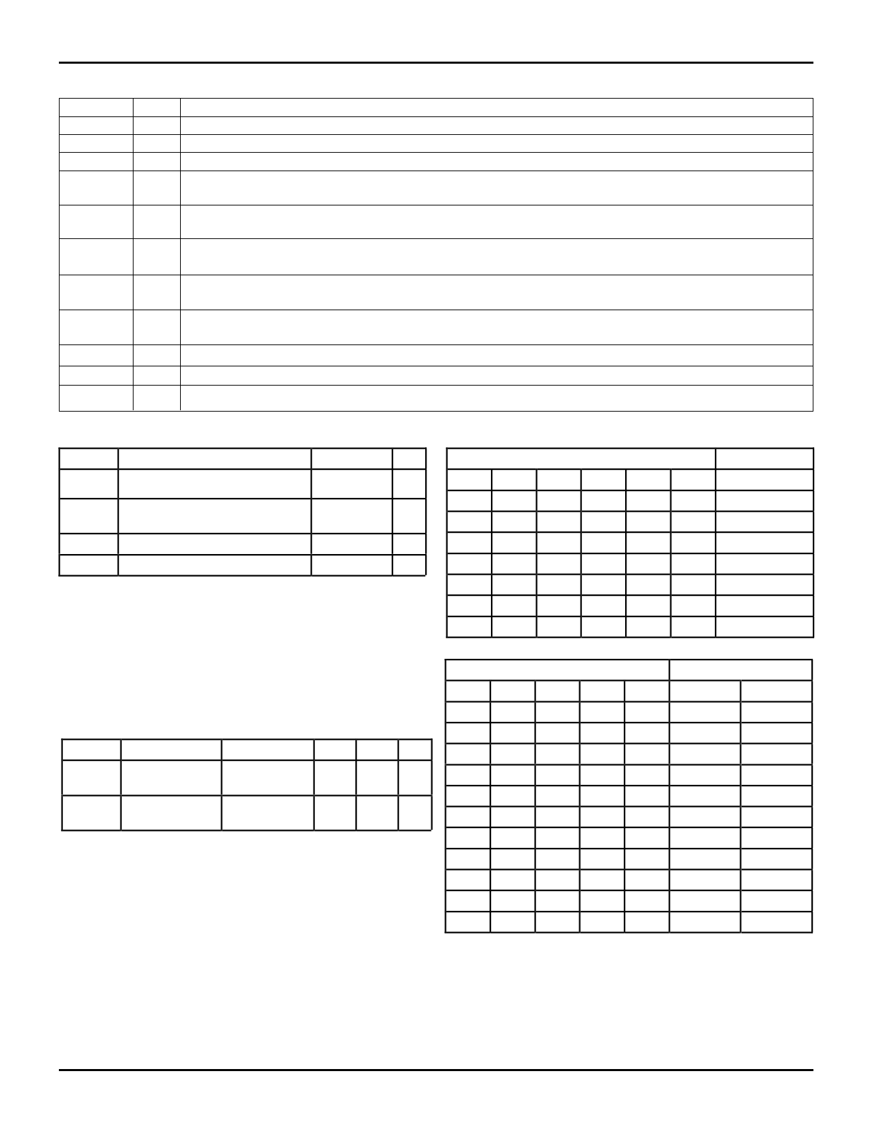
PIN DESCRIPTION
Signal
A(1:12)
1B(1:12)
2B(1:12)
LEA1B
LEA2B
LE1B
LE2B
SEL
OEA
OE1B
OE2B
I/O
Description
I/O Bidirectional Data Port A. Usually connected to the CPU's Address/Data bus.
I/O Bidirectional Data Port 1B. Connected to the even path or even bank of memory.
I/O Bidirectional Data Port 2B. Connected to the odd path or odd bank of memory.
I Latch Enable Input for A-1B Latch. The Latch is open when LEA1B is HIGH. Data from the A-port is latched on
the HIGH to LOW transition of LEA1B.
I Latch Enable Input for A-2B Latch. The Latch is open when LEA2B is HIGH. Data from the A-Port is latched on
the HIGH to LOW transition of LEA2B.
I Latch Enable Input for the 1B-A Latch. The Latch is open when LE1B is HIGH. Data from the 1B port is latched
on the HIGH to LOW transition of LE1B.
I Latch Enable Input for the 2B-A Latch. The Latch is open when LE2B is HIGH. Data from the 2B port is latched
on the HIGH to LOW transition of LE2B.
I 1B or 2B Path Selection. When HIGH, SEL enables data transfer from 1B Port to A Port. When LOW, SEL enables
data transfer from 2B Port to A Port.
I Output Enable for A Port (Active LOW).
I Output Enable for 1B Port (Active LOW).
I Output Enable for 2B Port (Active LOW).
ABSOLUTE MAXIMUM RATINGS(1)
FUNCTION TABLES(2)
3032 tbl 01
Symbol
Description
VTERM(2) Terminal Voltage with Respect to
GND
VTERM(3) Terminal Voltage with Respect to
GND
TSTG Storage Temperature
Max.
–0.5 to +7.0
–0.5 to
VCC +0.5
–65 to +150
Unit
V
V
°C
Inputs
1B 2B SEL LE1B LE2B OEA
H
X
H
H
X
L
L
X
H
H
X
L
X
X
H
L
X
L
Output
A
H
L
A(1)
IOUT
DC Output Current
–60 to +120 mA
NOTES:
3032 tbl 02
1. Stresses greater than those listed under ABSOLUTE MAXIMUM RAT-
INGS may cause permanent damage to the device. This is a stress rating
only and functional operation of the device at these or any other conditions
above those indicated in the operational sections of this specification is
not implied. Exposure to absolute maximum rating conditions for
extended periods may affect reliability.
2. All device terminals except FCT162XXXT Output and I/O terminals.
3. Output and I/O terminals for FCT162XXXT.
X
H
L
X
H
X
L
L
X
H
X
X
L
X
L
X
X
X
X
X
Inputs
A LEA1B LEA2B OE1B OE2B
L
H
L
L
L
A(1)
H
Z
3032 tbl 04
Outputs
1B
2B
CAPACITANCE (TA = +25°C, F = 1.0MHZ)
H
H
H
L
L
H
H
L
H
H
L
L
L
L
Symbol Parameter(1) Conditions Typ. Max. Unit
H
H
L
L
L
H
B(1)
CIN
Input
VIN = 0V
3.5 6.0 pF
L
H
L
L
L
L
B(1)
Capacitance
H
L
H
L
L
B(1)
H
CI/O
I/O
VOUT = 0V 3.5 8.0 pF
Capacitance
L
L
H
L
L
B(1)
L
NOTE:
3032 tbl 03
X
L
L
L
L
B(1)
B(1)
1. This parameter is measured at characterization but not tested.
X
X
X
H
H
Z
Z
X
X
X
L
H
Active
Z
X
X
X
H
L
Z
Active
X
X
X
L
L
Active
Active
NOTES:
3032 tbl 05
1. Output level before the indicated steady-state input conditions were
established.
2. H = HIGH Voltage Level
L = LOW Voltage Level
X = Don't Care
Z = High Impedance
↑ = LOW-to-HIGH Transition
5.4
3
Share Link: 