IH5352CBP 데이터 시트보기 (PDF) - Intersil
부품명
상세내역
제조사
IH5352CBP Datasheet PDF : 8 Pages
| |||
IH5352
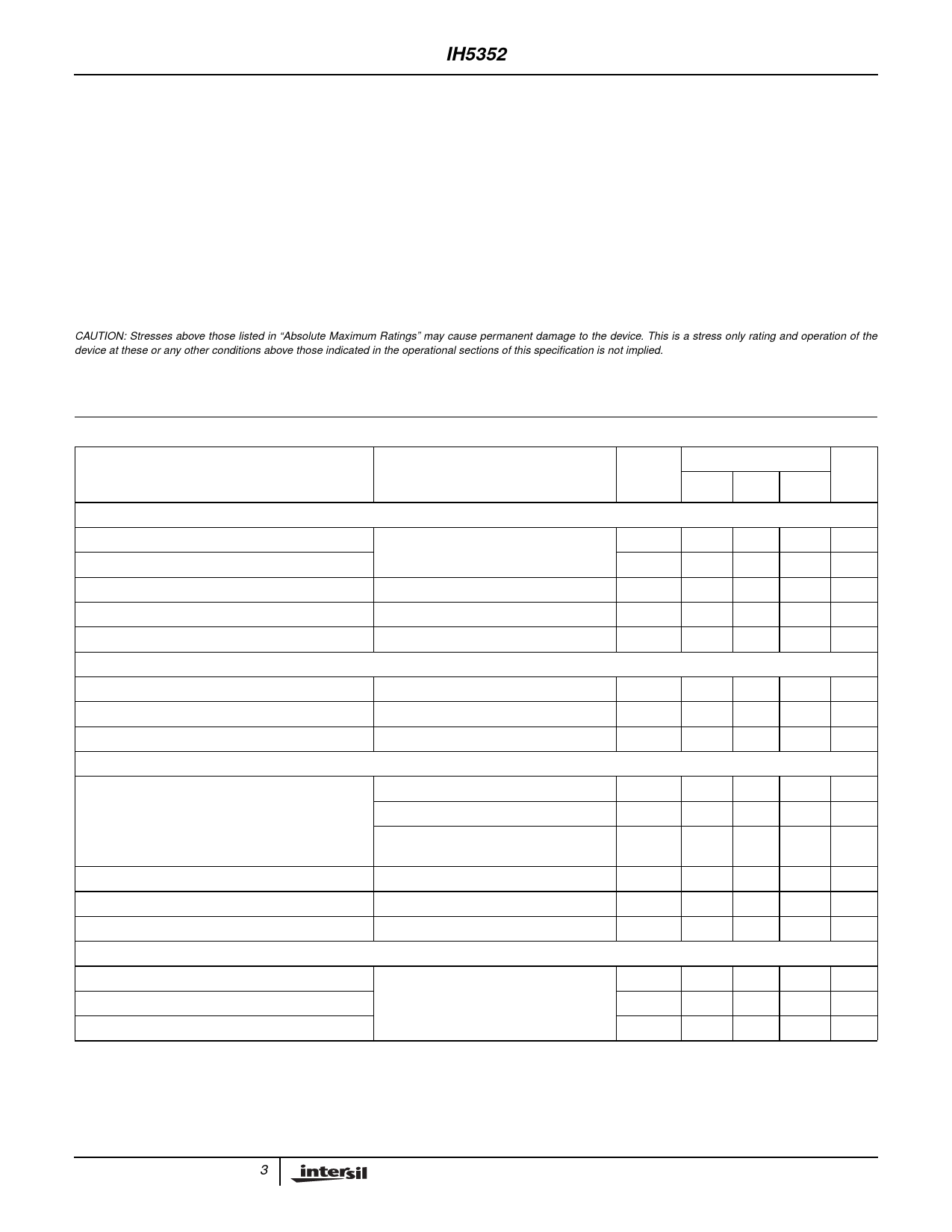
Absolute Maximum Ratings
V+ to Ground . . . . . . . . . . . . . . . . . . . . . . . . . . . . . . . . . . . . . . +18V
V- to Ground. . . . . . . . . . . . . . . . . . . . . . . . . . . . . . . . . . . . . . . . -18V
VL to Ground . . . . . . . . . . . . . . . . . . . . . . . . . . . . . . . . . . . . V+ to V-
Logic Control Voltage. . . . . . . . . . . . . . . . . . . . . . . . . . . . . . V+ to V-
Analog Input Voltage . . . . . . . . . . . . . . . . . . . . . . . . . . . . . . V+ to V-
Current (Any Terminal). . . . . . . . . . . . . . . . . . . . . . . . . . . . . . . 50mA
Operating Conditions
Temperature Range . . . . . . . . . . . . . . . . . . . . . . . . . . . 0oC to 70oC
Supply Voltage Range
V+, VL. . . . . . . . . . . . . . . . . . . . . . . . . . . . . . . . . . . . . . 5V to 15V
V- . . . . . . . . . . . . . . . . . . . . . . . . . . . . . . . . . . . . . . . . -5V to -15V
Thermal Information
Thermal Resistance (Typical, Note 1)
θJA (oC/W)
SOIC Package . . . . . . . . . . . . . . . . . . . . . . . . . . . . .
90
PDIP Package . . . . . . . . . . . . . . . . . . . . . . . . . . . . .
90
Maximum Junction Temperature (Plastic Packages) . . . . . . .150oC
Maximum Storage Temperature Range . . . . . . . . . . -65oC to 150oC
Maximum Lead Temperature (Soldering, 10s). . . . . . . . . . . . 300oC
(SOIC - Lead Tips Only)
CAUTION: Stresses above those listed in “Absolute Maximum Ratings” may cause permanent damage to the device. This is a stress only rating and operation of the
device at these or any other conditions above those indicated in the operational sections of this specification is not implied.
NOTE:
1. θJA is measured with the component mounted on an evaluation PC board in free air.
Electrical Specifications V+ = +15V, VL = +5V, V- = -15V, Unless Otherwise Specified
PARAMETER
TEST CONDITIONS
(NOTE 2)
TYP
25oC
DYNAMIC CHARACTERISTICS
Turn ON Time, tON
Figure 1
150
Turn OFF Time, tOFF
80
OFF Isolation, OIRR
Figure 2
70
Crosstalk, CCRR
Figure 3
-60
Switch Attenuation 3dB Frequency, f3dB
Figure 4
100
DIGITAL INPUT CHARACTERISTICS
Logic “1” Input Voltage, VIH
Logic “0” Input Voltage, VIL
Input Logic Current, IIN
ANALOG SWITCH CHARACTERISTICS
VIN > 2.4V or < 0V
>2.4
<0.8
0.1
Drain-Source ON Resistance, rDS(ON)
VD = ±5V, IS = 10mA, VIN ≥ 2.4V
50
VD = ±10V, IS = 10mA, VIN ≥ 2.4V
100
V+ = VL = +5V, VIN = 3V, V- = -5V,
175
VD = ±3V, IS = 10mA
On Resistance Match Between Channels, ∆rDS(ON) IS = 10mA, VD = ±5V
5
Switch OFF Leakage Current, ID(OFF) or IS(OFF)
VS/D = ±5V or ±14V, VIN ≤ 0.8V (Note 3)
-
Switch ON Leakage Current, ID(ON) + IS(ON)
VS/D = ±5V or ±14V, VIN ≥ 2.4V
-
POWER SUPPLY CHARACTERISTICS
Positive Supply Quiescent Current, I+
VIN = 0V or +5V
0.1
Negative Supply Quiescent Current, I-
0.1
Logic Supply Quiescent Current, IL
0.1
NOTES:
2. Typical values are not tested in production. They are given as a design aid only.
3. Positive and negative voltages applied to opposite sides of switch, in both directions successively.
4. Min or Max value, unless otherwise specified.
(NOTE 4)
0oC 25oC 70oC UNITS
-
-
-
ns
-
-
-
ns
-
-
-
dB
-
-
-
dB
-
-
-
MHz
-
-
-
V
-
-
-
V
±1
±1
10
µA
75
75 100
Ω
150 150 175
Ω
300 300 350
Ω
-
-
-
Ω
-
±2
100
nA
-
±2
100
nA
1
1
10
µA
1
1
10
µA
1
1
10
µA
3
Share Link: 