KM4101 데이터 시트보기 (PDF) - Fairchild Semiconductor
부품명
상세내역
제조사
KM4101 Datasheet PDF : 11 Pages
| |||
KM4100/KM4101
DATA SHEET
General Description
The KM4100/KM4101 are single supply, general
purpose, voltage-feedback amplifiers fabricated on a
complementary bipolar process using a patent pending
topology. They feature a rail-to-rail output stage and
are unity gain stable. Both gain bandwidth and slew
rate are insensitive to temperature.
The common mode input range extends to 300mV
below ground and to 1.2V below Vs. Exceeding these
values will not cause phase reversal. However, if the
input voltage exceeds the rails by more than 0.5V, the
input ESD devices will begin to conduct. The output
will stay at the rail during this overdrive condition.
The design uses a Darlington output stage. The output
stage is short circuit protected and offers “soft”
saturation protection that improves recovery time.
The typical circuit schematic is shown in Figure 1.
+Vs
6.8µF
+
In
0.01µF
+
Out
KM4100
-
Rf
Rg
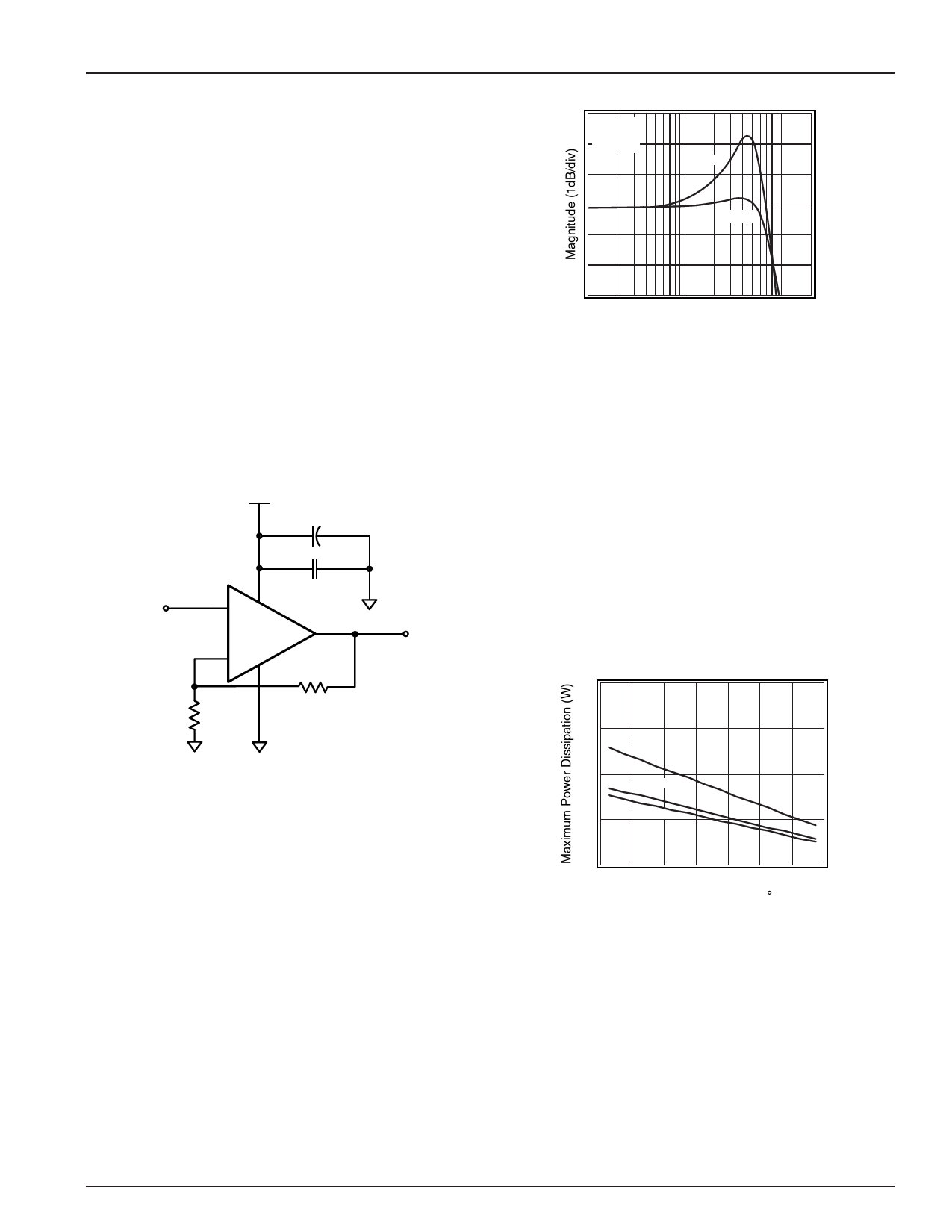
Frequency Reponse vs. Rf
G=2
RL = 2kΩ
Vs = +5V
Rf = 2kΩ
Rf = 1kΩ
1
10
100
Frequency (MHz)
Figure 2: Frequency Response vs. Rf
Power Dissipation
The maximum internal power dissipation allowed is
directly related to the maximum junction temperature.
If the maximum junction temperature exceeds 150°C,
some reliability degradation will occur. If the maximum
junction temperature exceeds 175°C for an extended
time, device failure may occur.
The KM4100/KM4101 are short circuit protected.
However, this may not guarantee that the maximum
junction temperature (+150°C) is not exceeded under
all conditions. Follow the maximum power derating
curves shown in Figure 3 to ensure proper operation.
Maximum Power Dissipation
2.0
1.5
SOIC-8 lead
Figure 1: Typical Configuration
At non-inverting gains other than G = +1, keep Rg
below 1kΩ to minimize peaking; thus, for optimum
response at a gain of +2, a feedback resistor of 1kΩ is
recommended. Figure 2 illustrates the KM4100/
KM4101 frequency response with both 1kΩ and 2kΩ
feedback resistors.
Enable/Disable Function (KM4101)
The KM4101 offers an active-low disable pin that can
be used to lower its supply current. Leave the pin
floating to enable the part. Pull the disable pin to the
negative supply (which is ground in a single supply
application) to disable the output. During the disable
condition, the nominal supply current will drop to
below 127µA and the output will be at high impedance
with about 2pF capacitance.
1.0
SOT23-6 lead
0.5 SOT23-5 lead
0
-50 -30 -10 10 30 50 70 90
Ambient Temperature ( C)
Figure 3: Power Derating Curves
Overdrive Recovery
For an amplifier, an overdrive condition occurs when
the output and/or input ranges are exceeded. The
recovery time varies based on whether the input or
output is overdriven and by how much the ranges are
exceeded. The KM4100/KM4101 will typically recover
in less than 20ns from an overdrive condition. Figure
4 shows the KM4100 in an overdriven condition.
REV. 1A February 2001
7
Share Link: 