LH28F800BG-L 데이터 시트보기 (PDF) - Sharp Electronics
부품명
상세내역
제조사
LH28F800BG-L Datasheet PDF : 43 Pages
| |||
The CUI does not occupy an addressable memory
location. It is written when WE# and CE# are
active. The address and data needed to execute a
command are latched on the rising edge of WE# or
CE# (whichever goes high first). Standard
microprocessor write timings are used. Fig. 12 and
Fig. 13 illustrate WE# and CE# controlled write
operations.
LH28F800BG-L/BGH-L (FOR TSOP, CSP)
4 COMMAND DEFINITIONS
When the VPP voltage ≤ VPPLK, read operations
from the status register, identifier codes, or blocks
are enabled. Placing VPPH1/2/3 on VPP enables
successful block erase and word write operations.
Device operations are selected by writing specific
commands into the CUI. Table 3 defines these
commands.
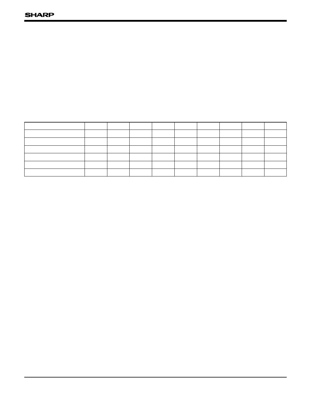
Table 2 Bus Operations
MODE
Read
Output Disable
NOTE RP#
1, 2, 3, 8 VIH or VHH
3 VIH or VHH
CE#
VIL
VIL
OE#
VIL
VIH
WE# ADDRESS VPP
VIH
X
X
VIH
X
X
DQ0-15
DOUT
High Z
RY/BY#
X
X
Standby
Deep Power-Down
3 VIH or VHH VIH
X
X
X
X High Z X
4
VIL
X
X
X
X
X
High Z VOH
Read Identifier Codes
8 VIH or VHH VIL
VIL
VIH See Fig. 2 X (NOTE 5) VOH
Write
3, 6, 7, 8 VIH or VHH VIL
VIH
VIL
X
X
DIN
X
NOTES :
1. Refer to Section 6.2.3 "DC CHARACTERISTICS".
When VPP ≤ VPPLK, memory contents can be read, but
not altered.
2. X can be VIL or VIH for control pins and addresses, and
VPPLK or VPPH1/2/3 for VPP. See Section 6.2.3 "DC
CHARACTERISTICS" for VPPLK and VPPH1/2/3 voltages.
3. RY/BY# is VOL when the WSM is executing internal
block erase or word write algorithms. It is VOH during
when the WSM is not busy, in block erase suspend
mode (with word write inactive), word write suspend
mode or deep power-down mode.
4. RP# at GND±0.2 V ensures the lowest deep power-
down current.
5. See Section 4.2 for read identifier code data.
6. Command writes involving block erase or word write are
reliably executed when VPP = VPPH1/2/3 and VCC =
VCC1/2/3/4. Block erase or word write with VIH < RP# <
VHH produce spurious results and should not be
attempted.
7. Refer to Table 3 for valid DIN during a write operation.
8. Don’t use the timing both OE# and WE# are VIL.
- 10 -
Share Link: 