M24C64-WMW6 데이터 시트보기 (PDF) - STMicroelectronics
부품명
상세내역
제조사
M24C64-WMW6 Datasheet PDF : 19 Pages
| |||
M24C64, M24C32
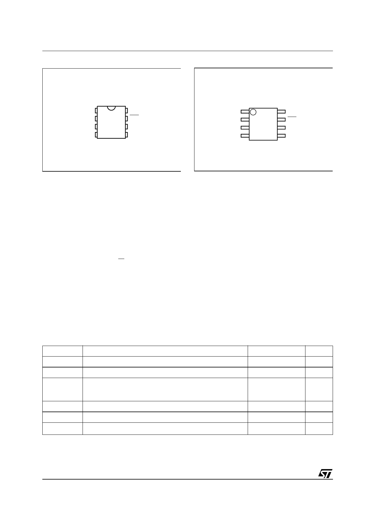
Figure 2A. DIP Connections
M24C64
M24C32
E0 1
E1 2
8 VCC
7 WC
E2 3
6 SCL
VSS 4
5 SDA
AI01845B
Figure 2B. SO and TSSOP Connections
E0
E1
E2
VSS
M24C64
M24C32
1
8
2
7
3
6
4
5
AI01846B
VCC
WC
SCL
SDA
These memory devices are compatible with the
I2C extended memory standard. This is a two wire
serial interface that uses a bi-directional data bus
and serial clock. The memory carries a built-in 4-
bit unique Device Type Identifier code (1010) in
accordance with the I2C bus definition.
The memory behaves as a slave device in the I2C
protocol, with all memory operations synchronized
by the serial clock. Read and Write operations are
initiated by a START condition, generated by the
bus master. The START condition is followed by a
Device Select Code and RW bit (as described in
Table 3), terminated by an acknowledge bit.
When writing data to the memory, the memory in-
serts an acknowledge bit during the 9th bit time,
following the bus master’s 8-bit transmission.
When data is read by the bus master, the bus
master acknowledges the receipt of the data byte
in the same way. Data transfers are terminated by
a STOP condition after an Ack for WRITE, and af-
ter a NoAck for READ.
Power On Reset: VCC Lock-Out Write Protect
In order to prevent data corruption and inadvertent
write operations during power up, a Power On Re-
set (POR) circuit is included. The internal reset is
held active until the VCC voltage has reached the
POR threshold value, and all operations are dis-
abled – the device will not respond to any com-
mand. In the same way, when VCC drops from the
operating voltage, below the POR threshold value,
all operations are disabled and the device will not
respond to any command. A stable and valid VCC
must be applied before applying any logic signal.
SIGNAL DESCRIPTION
Serial Clock (SCL)
The SCL input pin is used to strobe all data in and
out of the memory. In applications where this line
is used by slaves to synchronize the bus to a slow-
Table 2. Absolute Maximum Ratings 1
Symbol
Parameter
Value
Unit
TA
Ambient Operating Temperature
-40 to 125
°C
TSTG
Storage Temperature
-65 to 150
°C
PSDIP8: 10 seconds
260
TLEAD
Lead Temperature during Soldering
SO8: 40 seconds
215
°C
TSSOP8: 40 seconds
215
VIO
Input or Output range
-0.6 to 6.5
V
VCC
Supply Voltage
-0.3 to 6.5
V
VESD
Electrostatic Discharge Voltage (Human Body model) 2
4000
V
Note: 1. Except for the rating “Operating Temperature Range”, stresses above those listed in the Table “Absolute Maximum Ratings” may
cause permanent damage to the device. These are stress ratings only, and operation of the device at these or any other conditions
above those indicated in the Operating sections of this specification is not implied. Exposure to Absolute Maximum Rating condi-
tions for extended periods may affect device reliability. Refer also to the ST SURE Program and other relevant quality documents.
2. MIL-STD-883C, 3015.7 (100 pF, 1500 Ω)
2/19
Share Link: 