MAX17409 데이터 시트보기 (PDF) - Maxim Integrated
부품명
상세내역
제조사
MAX17409 Datasheet PDF : 32 Pages
| |||
1-Phase Quick-PWM GPU Controller
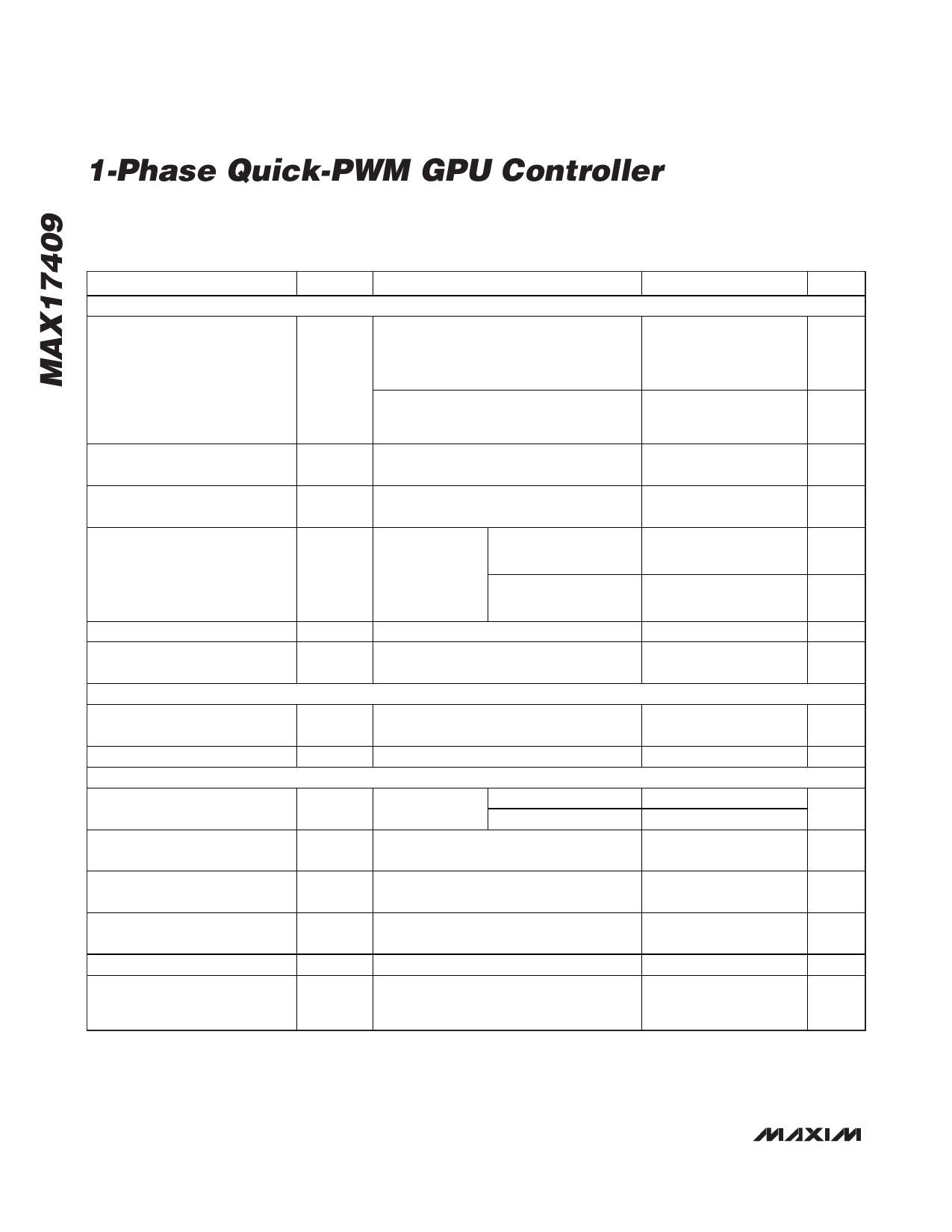
ELECTRICAL CHARACTERISTICS (continued)
(Circuit of Figure 1, VIN = 12V, VDD = VCC = 5V, SHDN = ILIM = VCC, SKIP = GNDS = PGND = GND, VFB = VCSP = VCSN = 1.05V;
G5–G0 set for 1.05V (G0–G5 = 100110); TA = -40°C to +105°C, unless otherwise specified.) (Note 3)
PARAMETER
FAULT PROTECTION
Output Overvoltage-Protection
Threshold
Output Undervoltage-Protection
Threshold
SYMBOL
CONDITIONS
VOVP
VUVP
Skip mode after output reaches the
regulation voltage or PWM mode;
measured at FB with respect to unloaded
output voltage
Soft-start, soft-shutdown, skip mode, and
output have not reached the regulation
voltage, measured at FB
Measured at FB with respect to unloaded
output voltage
MIN
250
1.45
-450
TYP MAX UNITS
350
mV
1.55
V
-350
mV
PWRGD Startup Delay
Measured at startup from the time when
SHDN goes high
3
8
ms
PWRGD Threshold
Measured at FB
with respect to
unloaded output
voltage; 15mV
hysteresis (typ)
Lower threshold, falling
edge (undervoltage)
Upper threshold, rising
edge (overvoltage)
-350
+150
-250
mV
+250 mV
PWRGD Output Low Voltage
ISINK = 3mA
VCC Undervoltage-Lockout
Threshold
VUVLO(VCC)
Rising edge, 50mV typical hysteresis,
controller disabled below this level
THERMAL COMPARATOR AND PROTECTION
VRHOT Trip Threshold
Measured at THRM with respect to VCC;
falling edge; typical hysteresis = 100mV
VRHOT Output On-Resistance
RVRHOT Low state
VALLEY CURRENT LIMIT AND DROOP
Current-Limit Threshold Voltage
(Positive Adjustable)
VLIMIT VCSP - VCSN
VREF - VILIM = 100mV
VREF - VILIM = 500mV
Current-Limit Threshold Voltage
(Positive Default)
ILIM = VCC, VCSP - VCSN
4.0
29.2
7
45
20
0.4
V
4.5
V
30.8
%
8
13
mV
55
25
mV
Current-Limit Threshold Voltage
(Negative) Accuracy
VLIMIT(NEG) VCSP - VCSN, nominally -125% of VLIMIT
-5
+5
mV
CSP, CSN Common-Mode
Input Range
Droop Amplifier GMD) Offset
Droop Amplifier (GMD)
Transconductance
0
(VCSP - VCSN) at IFB = 0
-1.0
IFB/(VCSP - VCSN);
FB = CSN = 0.45V to 2.0V,
588
and (VCSP - VCSN) = -15.0mV to +15.0mV
1.9
V
+1.0
mV
612
µS
6 _______________________________________________________________________________________
Share Link: 