MAX2204 데이터 시트보기 (PDF) - Maxim Integrated
부품명
상세내역
제조사
MAX2204 Datasheet PDF : 7 Pages
| |||

RF Power Detector
ABSOLUTE MAXIMUM RATINGS
VCC to GND ...........................................................-0.3V to +3.6V
OUT, Logic Input (ENA) to GND ................-0.3V to (VCC + 0.3V)
RF Input Power ...............................................................+10dBm
Continuous Power Dissipation (TA = +70°C)
(derate 3.1mW/°C above +70°C) ................................247mW
Operating Temperature Range ...........................-40°C to +85°C
Junction Temperature ......................................................+150°C
θJC ...............................................................................+115°C/W
θJA ...............................................................................+324°C/W
Storage Temperature Range .............................-65°C to +160°C
Lead Temperature (soldering, 10s) .................................+300°C
Stresses beyond those listed under “Absolute Maximum Ratings” may cause permanent damage to the device. These are stress ratings only, and functional
operation of the device at these or any other conditions beyond those indicated in the operational sections of the specifications is not implied. Exposure to
absolute maximum rating conditions for extended periods may affect device reliability.
CAUTION! ESD SENSITIVE DEVICE
Note: This part is not for automotive applications.
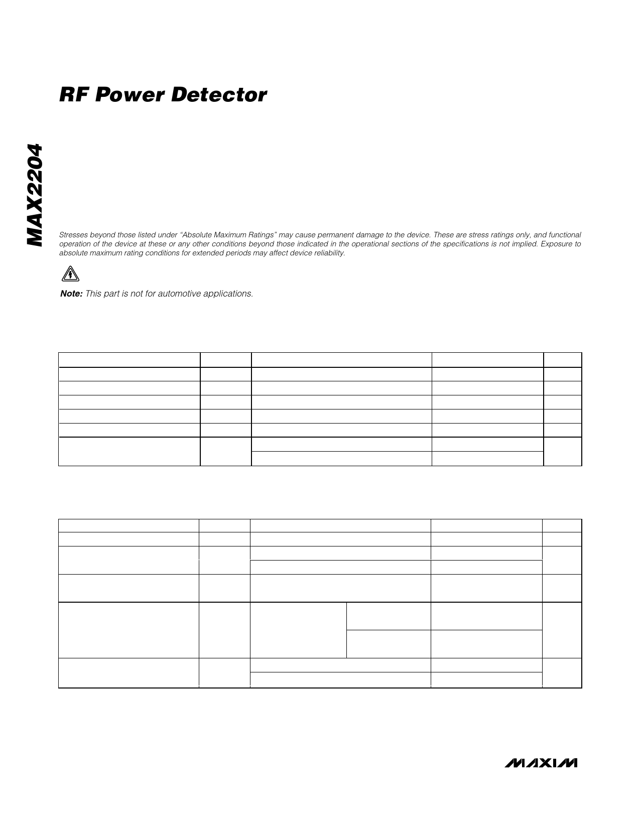
DC ELECTRICAL CHARACTERISTICS
(VCC = 2.7V to 3.3V, TA = -40°C to +85°C, ENA = 2.0V, no RF signal applied. Typical values are at VCC = 2.85V, TA = +25°C, unless
otherwise noted.) (Note 1)
PARAMETER
Supply Voltage
Operating Supply Current
Sleep Mode Supply Current
ENA Logic-High Threshold
ENA Logic-Low Threshold
ENA Input Current
SYMBOL
VCC
ICC
VIH
VIL
ENA = 0V
ENA = 2V
ENA = 0.6V
CONDITIONS
MIN TYP MAX UNITS
2.7
3.3
V
1.2
2.5
mA
0.5
10
µA
2
V
0.6
V
-2
+10
µA
-2
+1
AC ELECTRICAL CHARACTERISTICS
(MAX2204 Evaluation Kit, VCC = 2.85V, TA = -40°C to +85°C, ENA = 2.0V. fRF = 450MHz to 2.5GHz. Typical values are at VCC = 2.85V,
TA =+25°C, unless otherwise noted.) (Note 1)
PARAMETER
SYMBOL
CONDITIONS
MIN TYP MAX UNITS
RF Input Frequency
450
2500 MHz
RF Input Level for 2.0V
TA = +25°C, RFIN at 836MHz
TA = +25°C, RFIN at 1880MHz
3.3
4.8
6.3
dBm
1.9
3.4
4.9
Minimum Input Level
-16dBm to -15dBm change in PIN
(836MHz to 2500MHz)
8
14
mV
Power Detector Accuracy Due to
Temperature
VCC = 2.85V,
836MHz to 1880MHz
TA = -40°C to +85°C
(Note 2)
PIN for 2.0V output
PIN for 0.1V output
±0.5 ±1.1
dB
±1.5
±4
In-Band Variation
824MHz to 849MHz
1850MHz to 1980MHz
0.1
dB
0.2
Note 1: Specifications over TA = -40°C to +85°C are guaranteed by design. Production tests are performed at TA = +25°C.
Note 2: Guaranteed by design and characterization.
2 _______________________________________________________________________________________