MAX3509 데이터 시트보기 (PDF) - Maxim Integrated
부품명
상세내역
제조사
MAX3509 Datasheet PDF : 10 Pages
| |||
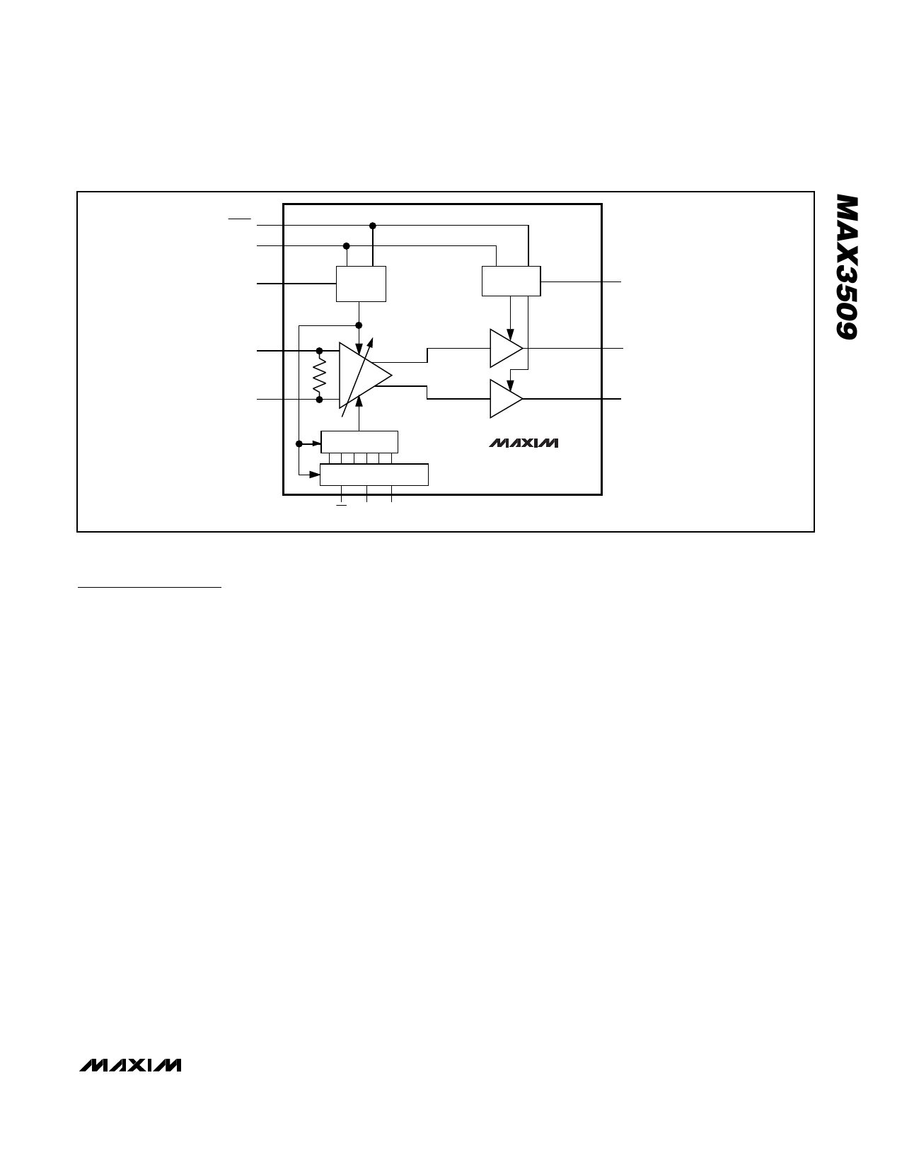
Upstream CATV Amplifier
SHDN
TXEN
VCC1
PGA BIAS
PA BIAS
VCC2
IN+
OUT+
IN-
OUT-
DAC
SERIAL DATA INTERFACE
CS SDA SCLK
Figure 1. MAX3509 Functional Diagram
Detailed Description
The following sections describe the blocks shown in the
functional diagram (Figure 1).
Programmable-Gain Amplifier
The PGA consists of the variable-gain amplifier (VGA)
and the digital-to-analog converter (DAC), which pro-
vide better than 55dB of output level control in 1dB
steps.
The PGA is implemented as a programmable Gilbert-
cell attenuator. It uses a differential architecture to
achieve maximum linearity. The gain of the PGA is
determined by a 6-bit word (D5–D0) programmed
through the serial data interface (Tables 1 and 2).
Specified performance is achieved when the input is
driven differentially. The device may be driven single
ended; however, a slight increase in even-order distor-
tion may result at low output levels. To drive the device
in this manner, one of the input pins must be capaci-
tively coupled to ground. Use a capacitor value large
enough to allow for a low-impedance path to ground at
the lowest frequency of operation.
Power Amplifier
The power amplifier has two current-feedback ampli-
fiers in an instrumentation amplifier configuration. This
architecture provides superior even-order distortion
performance but requires an external transformer to
MAX3509
convert to a single-ended output. In transmit-disable
mode, bias to the power amplifier is reduced to a mini-
mal level, which provides high input to output isolation
and low output noise.
Serial Interface
The serial interface has an active-low enable (CS) to
bracket the data, with data clocked in MSB first on the
rising edge of SCLK. Data is stored in the storage latch
on the rising edge of CS. The serial interface controls the
state of the PGA. Tables 1 and 2 show the register for-
mat. Serial-interface timing is shown in Figure 2.
PGA Bias Cell
The bias cell in the MAX3509 is controlled by the logic
levels present at TXEN and SHDN, as well as the pro-
gram state of D7, the MSB of the 8-bit program word.
Transmit-disable mode is actuated when the TXEN pin
is driven to a logic low or when D7 = 0. In this mode,
current to the PGA and power amps is reduced signifi-
cantly while maintaining normal current flow to the seri-
al data interface and DAC. This preserves the program
stored in the serial data interface.
A logic low at the SHDN pin overrides the state of the
TXEN pin or D7. In shutdown mode, the current to the
PGA, power amp, serial data interface, and DAC is cut
off, allowing only leakage currents to flow. The stored
gain control program is lost in this mode.
_______________________________________________________________________________________ 7
Share Link: 