MAX3658(2004) 데이터 시트보기 (PDF) - Maxim Integrated
부품명
상세내역
제조사
MAX3658 Datasheet PDF : 14 Pages
| |||
622Mbps, Low-Noise, High-Gain
Transimpedance Preamplifier
Select CCOUPLE so the low-frequency cutoff due to the
load resistors and coupling capacitors is much lower
than the low-frequency cutoff of the MAX3658. The cou-
pling capacitor should be 0.1µF or larger for SONET
data. For lowest jitter, 1.0µF is recommended. Refer to
application note HFAN-1.1: Choosing AC-Coupling
Capacitors for a more detailed discussion on choosing
AC-coupling capacitors.
Select Output Filter
Input sensitivity is improved by adding a filter between
TIA and the quantizer/limiting amplifier, with 0.5pF input
capacitance. Typical bandwidth of the MAX3658 is
580MHz; the highest expected bandwidth is 730MHz.
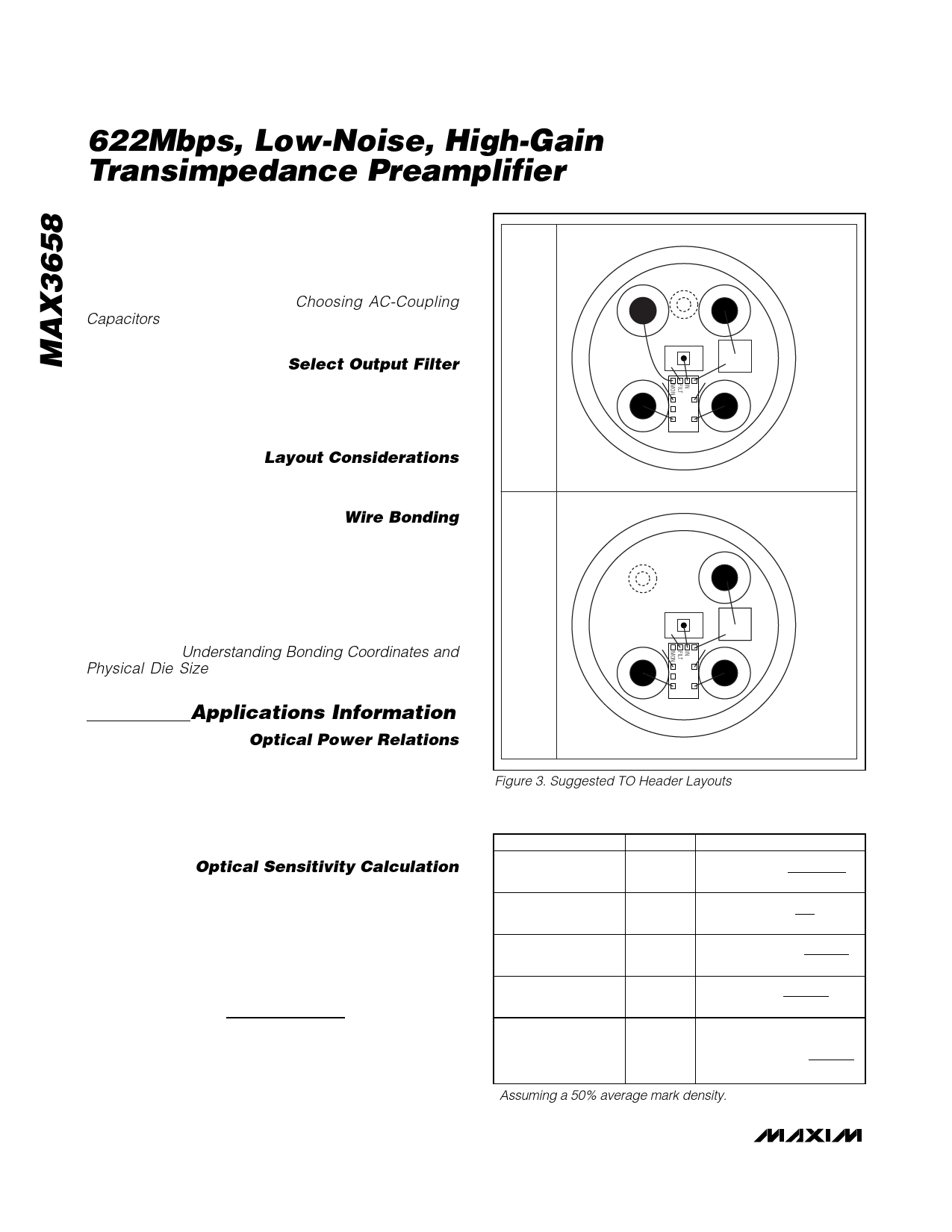
Layout Considerations
Figure 3 shows suggested layouts for 4- and 5-pin TO
headers.
Wire Bonding
For high-current density and reliable operation, the
MAX3658 uses gold metalization. For best results, use
gold-wire ball-bonding techniques. Use caution when
wedge bonding. Die-size is 52 mils x 29 mils, (1.32mm
x 0.736mm) and die thickness is 15 mils (380µm). The
bond-pad passivation opening is 75µm and bond-pad
metal thickness is 5µm. Refer to Maxim application note
HFAN-08.0.1: Understanding Bonding Coordinates and
Physical Die Size for additional information on bond-
pad coordinates.
Applications Information
Optical Power Relations
Many of the MAX3658 specifications relate to the input
signal amplitude. When working with optical receivers,
the input is sometimes expressed in terms of average
optical power and extinction ratio. Figure 4 and Table 1
show relations that are helpful for converting optical
power to input signal when designing with the MAX3658.
Optical Sensitivity Calculation
The input-referred RMS noise current (in) of the
MAX3658 generally determines the receiver sensitivity.
To obtain a system bit-error rate (BER) of 1E-10, the
signal-to-noise ratio must always exceed 12.7. The
input sensitivity, expressed in average power, can be
estimated as:
( ) SENSITIVITY
=
12.7
10log
×
in
×
re + 1
× 1000dBm
( ) 2 × ρ × re − 1
5-PIN HEADER
MON
OUT+
PHOTODIODE
VCC
CVCC2
OUT-
MAX3658A
PHOTODIODE
MOUNTED ON CFILT
OUTPUT POLARITIES
REVERSED FOR MAX3658B
CASE IS GROUND
4-PIN HEADER
CVCC2
VCC
PHOTODIODE
OUT+
OUT-
MAX3658A
PHOTODIODE
MOUNTED ON CFILT
OUTPUT POLARITIES
REVERSED FOR MAX3658B
CASE IS GROUND
Figure 3. Suggested TO Header Layouts
Table 1. Optical Power Relations*
PARAMETER
Average Power
SYMBOL
PAVG
RELATION
PAVG
=
P0 + P1
2
Extinction Ratio
re
Optical Power of a 1
P1
Optical Power of a 0
P0
Optical Modulation
Amplitude
PIN
re
=
P1
P0
P1
=
2PAVG
re
re
+
1
P0 = 2PAVG
re + 1
PIN = P1 − P0
=
2PAVG
re
re
−
+
1
1
*Assuming a 50% average mark density.
8 _______________________________________________________________________________________
Share Link: 