MAX3657(2004) 데이터 시트보기 (PDF) - Maxim Integrated
부품명
상세내역
제조사
MAX3657 Datasheet PDF : 15 Pages
| |||
155Mbps Low-Noise Transimpedance
Amplifier
AMPLITUDE
AMPLITUDE
INPUT FROM PHOTODIODE
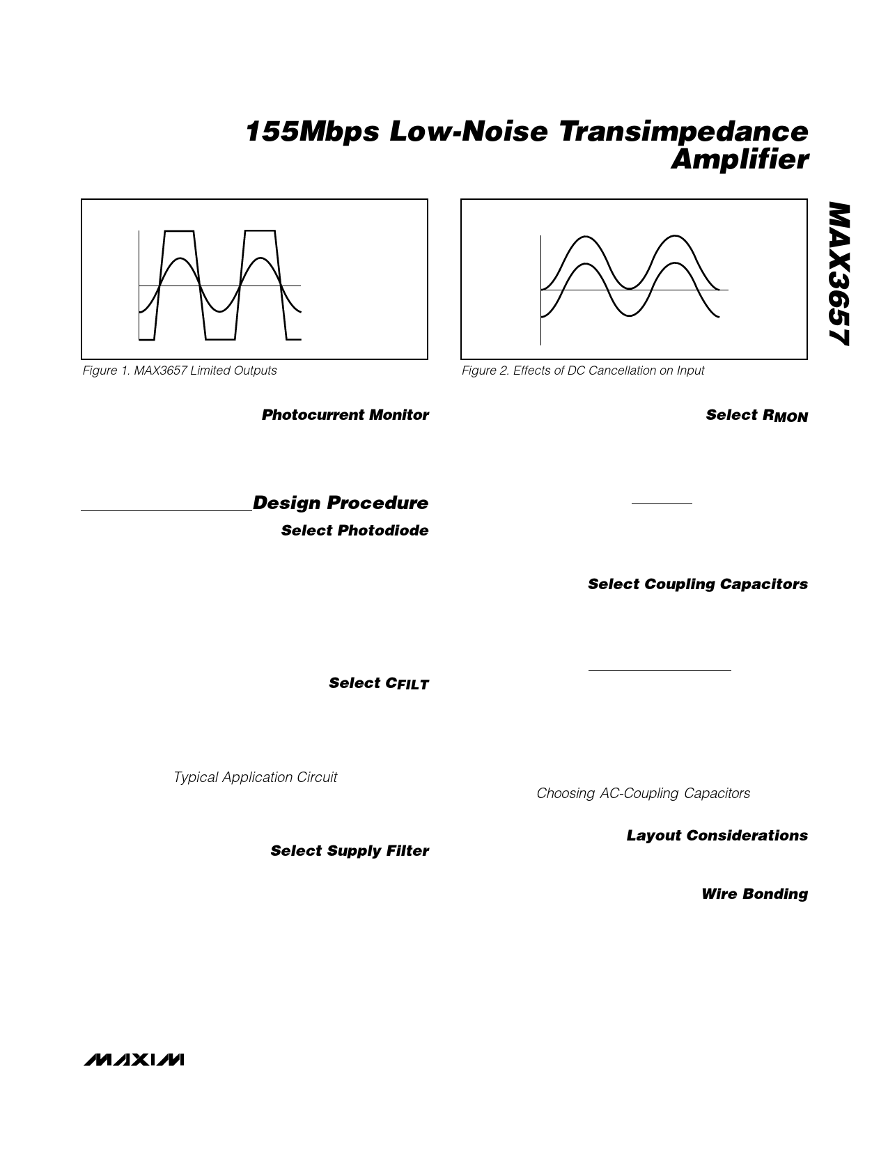
Figure 1. MAX3657 Limited Outputs
TIME
OUTPUT (SMALL SIGNALS)
OUTPUT (LARGE SIGNALS)
TIME
INPUT AFTER DC CANCELLATION
Figure 2. Effects of DC Cancellation on Input
Photocurrent Monitor
The MAX3657 includes an average photocurrent monitor.
The current at MON is approximately equal to the DC cur-
rent at IN. Best monitor accuracy is obtained when data
input edge time is longer than 500ps.
Design Procedure
Select Photodiode
Noise performance and bandwidth are adversely affected
by stray capacitance on the TIA input node. Select a
low-capacitance photodiode to minimize the total input
capacitance on this pin. The MAX3657 is optimized for
0.5pF of capacitance on the input. Assembling the
MAX3657 in die form using chip and wire technology
provides the lowest capacitance input and the best
possible performance.
Select CFILT
Supply voltage noise at the cathode of the photodiode
produces a current I = CPD ∆V/∆t, which reduces the
receiver sensitivity (CPD is the photodiode capaci-
tance). The filter resistor of the MAX3657, combined
with an external capacitor, can be used to reduce the
noise (see the Typical Application Circuit). Current gen-
erated by supply-noise voltage is divided between
CFILT and CPD. To obtain a good optical sensitivity,
select CFILT > 400pF.
Select Supply Filter
The MAX3657 requires wideband power-supply decou-
pling. Power-supply bypassing should provide low
impedance between VCC and ground for frequencies
between 10kHz and 200MHz. Use LC filtering at the
main supply terminal and decoupling capacitors as
close to the die as possible.
Select RMON
Connect a resistor between MON and ground to moni-
tor the average photocurrent. Select RMON as large as
possible:
RMON
=
2.1V
IMONMAX
where IMONMAX is the largest average input current
observed.
Select Coupling Capacitors
A receiver built with the MAX3657 has a bandpass fre-
quency response. The low-frequency cutoff due to the
coupling capacitors and load resistors is:
LFCTERM
=
2π
x
1
RLOAD x
CCOUPLE
Select CCOUPLE so the low-frequency cutoff due to the
load resistors and coupling capacitors is much lower than
the low-frequency cutoff of the MAX3657. The coupling
capacitor should be 0.1µF or larger, but 1.0µF is recom-
mended for lowest jitter. Refer to Maxim Application Note
HFAN-1.1: Choosing AC-Coupling Capacitors for more
information.
Layout Considerations
Figure 3 shows a suggested layout for a TO header for
the MAX3657.
Wire Bonding
For high-current density and reliable operation, the
MAX3657 uses gold metalization. For best results, use
gold-wire ball-bonding techniques. Use caution if
attempting wedge bonding. Die size is 41 mils x 48 mils,
(1040µm x 1220µm) and die thickness is 15 mils (380µm).
The bond pad is 94.4µm x 94.4µm and its metal thickness
is 1.2µm. Refer to Maxim Application Note HFAN- 8.0.1:
_______________________________________________________________________________________ 7
Share Link: 