MAX3815A 데이터 시트보기 (PDF) - Maxim Integrated
부품명
상세내역
제조사
MAX3815A Datasheet PDF : 11 Pages
| |||
TMDS Digital Video Equalizer for
HDMI/DVI Cables
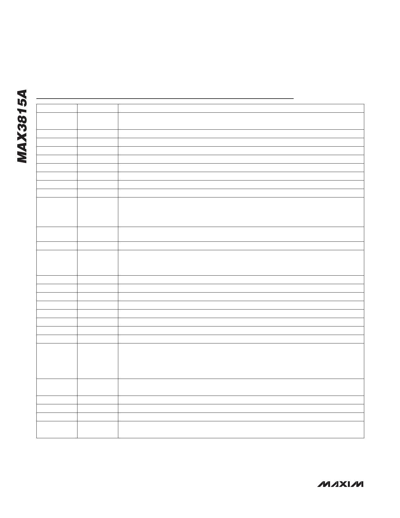
Pin Description
PIN
1, 4, 5, 8, 9,
12, 13, 16, 38
2
3
6
7
10
11
14
15
NAME
VCC
RX0_IN-
RX0_IN+
RX1_IN-
RX1_IN+
RX2_IN-
RX2_IN+
RXC_IN+
RXC_IN-
FUNCTION
Supply Voltage. All pins must be connected to VCC.
Negative Data Input, CML
Positive Data Input, CML
Negative Data Input, CML
Positive Data Input, CML
Negative Data Input, CML
Positive Data Input, CML
Positive Clock Input, CML
Negative Clock Input, CML
Equalizer Control. This pin allows the user to control the equalization level of the MAX3815A.
17
EQCONTROL
Connect the pin to GND for automatic operation. Set the voltage to VCC - 1V for minimum
equalization, or set the voltage between VCC - 1V and VCC for manual equalization. See the
Applications Information section for more information.
18
CLKLOS
Loss-of-Clock Signal Output, LVTTL Open Collector. This pin asserts low upon loss of the input
TMDS clock from the cable. Connect pin to VCC through a 4.7kω resistor.
19
N.C.
Not Connected. This pin is not internally connected.
20, 23, 24, 25,
28, 29, 32, 33,
36, 37
GND
Ground
21
RXC_OUT- Negative Clock Output, CML
22
RXC_OUT+ Positive Clock Output, CML
26
RX2_OUT+ Positive Data Output, CML
27
RX2_OUT- Negative Data Output, CML
30
RX1_OUT+ Positive Data Output, CML
31
RX1_OUT- Negative Data Output, CML
34
RX0_OUT+ Positive Data Output, CML
35
RX0_OUT- Negative Data Output, CML
Output-Level Control Input
• HIGH: Standard swing (1000mVP-P differential)
39
OUTLEVEL • OPEN: Standard swing (900mVP-P differential) with external 267ω back termination resistor
(see Figure 4)
• LOW: One-half standard swing (500mVP-P differential)
40
41, 43, 44
42
45–48
—
OUTON
VCC_T
GND_T
RES
EP
Output-Enable Control Input, LVTTL. This input enables the CML outputs when forced low and
sets a differential logic zero when forced high.
Reserved. Must be connected to VCC for normal operation.
Reserved. Must be connected to GND for normal operation.
Reserved. Must be left open for normal operation.
Exposed Pad. The exposed pad must be soldered to the circuit-board ground for proper
thermal and electrical operation.
6 _______________________________________________________________________________________
Share Link: 