MAX400 데이터 시트보기 (PDF) - Maxim Integrated
부품명
상세내역
제조사
MAX400 Datasheet PDF : 6 Pages
| |||
Ultra-Low Offset
Voltage Operational Amplifier
ABSOLUTE MAXIMUM RATINGS
Total Supply Voltage (V+ to V-) ...........................................±22V
Internal Power Dissipation.................................................500mV
TO-99 (T) (derate at 7.1mW/ above +80°C)
Hermatic Dip (J) (derate 6.7mW/°C above +75°C)
Plastic Dip (P) (derate 5.6mW/°C above +36°C)
Differential Input Voltage .....................................................±30V
Input Voltage (Note 1)..........................................................±22V
Storage Temperature Range .............................-65°C to +150°C
Operating Temperature Range
MAX400M ......................................................-55°C to +125°C
MAX400E .........................................................-40°C to +85°C
MAX400C ............................................................0°C to +70°C
Lead Temperature (soldering, 10s) .................................+300°C
Duration of Output Short Circuit ....................................Indefinite
Junction Temperature (TJ).................................-65°C to +160°C
Note 1: For supply voltages less than ±22V, the absolute maximum input voltage is equal to the supply voltage.
Stresses beyond those listed under “Absolute Maximum Ratings” may cause permanent damage to the device. These are stress ratings only, and functional
operation of the device at these or any other conditions beyond those indicated in the operational sections of the specifications is not implied. Exposure to
absolute maximum rating conditions for extended periods may affect device reliability.
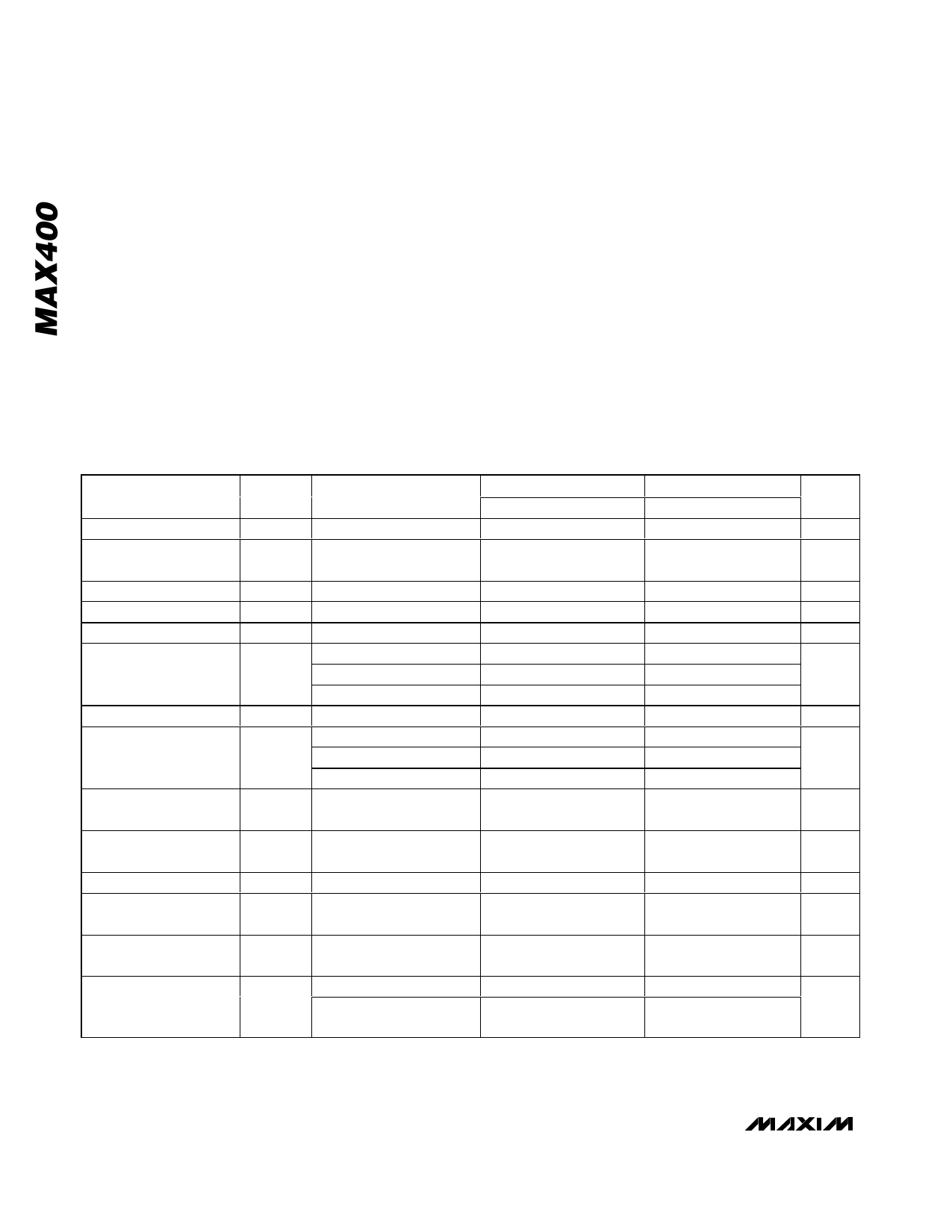
ELECTRICAL CHARACTERISTICS
(VS = ±15V, TA = +25°C, unless otherwise noted.)
PARAMETER
Input Offset Voltage
Long-Term Input Offset
Voltage Stability
Input Offset Current
Input Bias Current
Input Noise Voltage
Input Noise-Voltage
Density
Input Noise Current
Input Noise-Current
Density
Input Resistance
Differential Mode
SYMBOL
CONDITIONS
VOS (Note 2)
VOS/Time (Note 3)
IOS
IB
eN(P-P)
eN
IN(P-P)
IN
0.1Hz to 10Hz
fO = 10Hz
fO = 100Hz
fO = 1000Hz
0.1Hz to 10Hz
fO = 10Hz
fO = 100Hz
fO = 1000Hz
RIN (Note 4)
MAX400M
MIN TYP MAX
4
10
0.2
0.3
±0.7
0.35
10.3
10.0
9.6
14
0.32
0.14
0.12
2.0
±2.0
30
80
MAX400C/E
MIN TYP MAX
10
15
0.2
0.3
±0.7
0.35
10.3
10.0
9.6
14
0.32
0.14
0.12
2.0
±2.0
UNITS
µV
µV/
month
nA
nA
µVP-P
nV/√Hz
pAP-P
pA/√Hz
20
60
MΩ
Input Resistance
Common Mode
Input Voltage Range
Common-Mode
Rejection Ratio
RINCM
IVR
CMRR VCM = ±13V
200
200
GΩ
±13 ±14
±13 ±14
V
114 126
114 126
dB
Power-Supply Rejection
Ratio
Large-Signal Voltage
Gain
PSRR
AVO
VS = ±3V to ±18V
RL ≥ 2kΩ, VO = ±10V
RL ≥ 500Ω, VO = ±0.5V,
VS = ±3V (Note 4)
4
10
4
10
µV/V
500 1000
150 400
500 1000
150 400
V/mV
2 _______________________________________________________________________________________
Share Link: 