MAX4032 데이터 시트보기 (PDF) - Maxim Integrated
부품명
상세내역
제조사
MAX4032
Maxim Integrated

MAX4032 Datasheet PDF : 10 Pages
| |||
5V, 6dB Video Buffer with Sync-Tip Clamp,
Output Sag Correction, and 150nA Shutdown Current
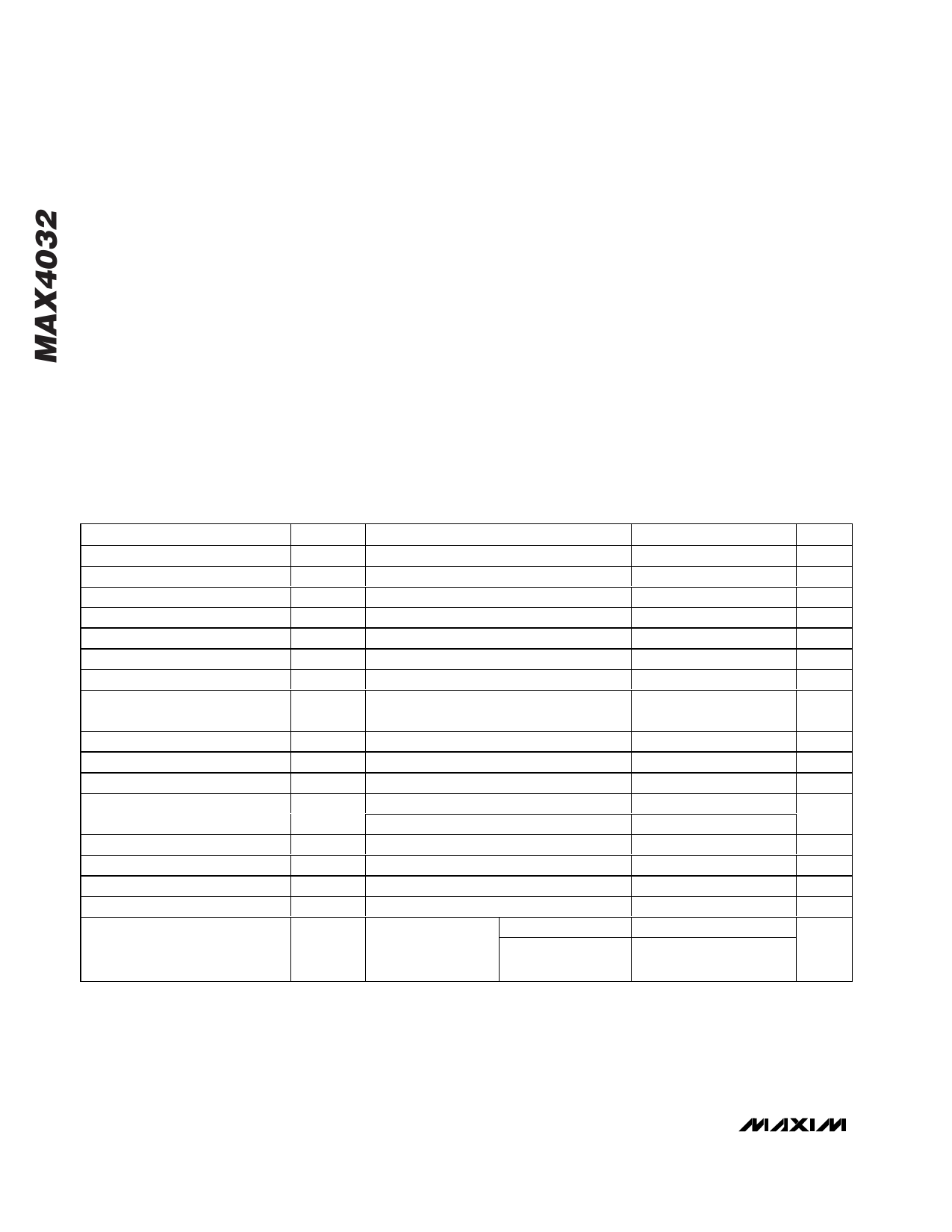
ABSOLUTE MAXIMUM RATINGS
VCC to GND ............................................................. -0.3V to +6V
OUT, SAG, SHDN to GND......................... -0.3V to (VCC + 0.3V)
IN to GND (Note 1) ................................... VCLP to (VCC + 0.3V)
IN Short-Circuit Duration from -0.3V to VCLP ........................1min
Output Short-Circuit Duration to VCC or GND .......... Continuous
Continuous Power Dissipation (TA = +70°C)
6-Pin SOT23 (derate 8.7mW/°C above +70°C) ...........695mW
6-Pin SC70 (derate 3.1mW/°C above +70°C) .............245mW
Operating Temperature Range ..........................-40°C to +85°C
Junction Temperature .....................................................+150°C
Storage Temperature Range ............................-65°C to +150°C
Lead Temperature (soldering, 10s) ................................+300°C
Note 1: VCLP is the input clamp voltage as defined in the DC Electrical Characteristics table.
Stresses beyond those listed under “Absolute Maximum Ratings” may cause permanent damage to the device. These are stress ratings only, and functional
operation of the device at these or any other conditions beyond those indicated in the operational sections of the specifications is not implied. Exposure to
absolute maximum rating conditions for extended periods may affect device reliability.
DC ELECTRICAL CHARACTERISTICS
(VCC = 5.0V, GND = 0V, CIN = 0.1µF from IN to GND, RL = infinity to GND, SAG shorted to OUT, SHDN = 5.0V, TA = -40°C to +85°C.
Typical values are at TA = +25°C, unless otherwise noted.) (Note 2)
PARAMETER
Supply Voltage Range
Quiescent Supply Current
Shutdown Supply Current
Input Clamp Voltage
Input Voltage Range
Input Bias Current
Input Resistance
Voltage Gain
SYMBOL
VCC
ICC
ISHDN
VCLP
VIN
IBIAS
AV
CONDITIONS
Guaranteed by PSRR
VIN = VCLP
SHDN = 0V
Input referred
Inferred from voltage gain (Note 3)
VIN = 1.45V
VCLP + 0.5V < VIN < VCLP + 1V
RL = 150Ω to GND, 0.5V < VIN < 1.45V
(Note 4)
MIN TYP MAX UNITS
4.5
5.5
V
6.5
10
mA
0.15
1
µA
0.27 0.38 0.47
V
VCLP
1.45
V
22.5
35
µA
3
MΩ
1.9
2
2.1
V/V
Power-Supply Rejection Ratio
Output Voltage High Swing
Output Voltage Low Swing
Output Current
Output Short-Circuit Current
SHDN Logic-Low Threshold
SHDN Logic-High Threshold
SHDN Input Current
Shutdown Output Impedance
PSRR
VOH
VOL
IOUT
ISC
VIL
VIH
IIH, IIL
ROUT
(Disabled)
4.5V < VCC < 5.5V
RL = 150Ω to GND
RL = 150Ω to GND
Sourcing, RL = 20Ω to GND
Sinking, RL = 20Ω to VCC
OUT shorted to VCC or GND
SHDN = 0V
At DC
At 3.58MHz or
4.43MHz
60
80
dB
4.3
4.6
V
VCLP 0.47
V
45
85
mA
40
85
110
mA
VCC x 0.7
VCC x 0.3
V
V
0.003
1
µA
4
kΩ
2
2 _______________________________________________________________________________________
Share Link: