MAX6633(2001) 데이터 시트보기 (PDF) - Maxim Integrated
부품명
상세내역
제조사
MAX6633
(Rev.:2001)
(Rev.:2001)
Maxim Integrated

MAX6633 Datasheet PDF : 16 Pages
| |||
12-Bit Plus Sign Temperature Sensors with
SMBus/I2C-Compatible Serial Interface
ABSOLUTE MAXIMUM RATINGS
VCC, SDA, SCL ......................................................-0.3V to +6.0V
All Other Pins ................................................-0.3V to VCC +0.3V
SDA, ALERT, OVERT Current .............................-1mA to +50mA
ESD Protection (Human Body Model)................................2000V
Continuous Power Dissipation (TA = +70°C)
8-Pin SO (derate 5.88mW/°C above +70°C)................471mW
Junction Temperature ......................................................+150°C
Operating Temperature Range .........................-55°C to +150°C
Storage Temperature Range .............................-65°C to +150°C
Lead Temperature (soldering, 10s) ................................+300°C
Stresses beyond those listed under “Absolute Maximum Ratings” may cause permanent damage to the device. These are stress ratings only, and functional
operation of the device at these or any other conditions beyond those indicated in the operational sections of the specifications is not implied. Exposure to
absolute maximum rating conditions for extended periods may affect device reliability.
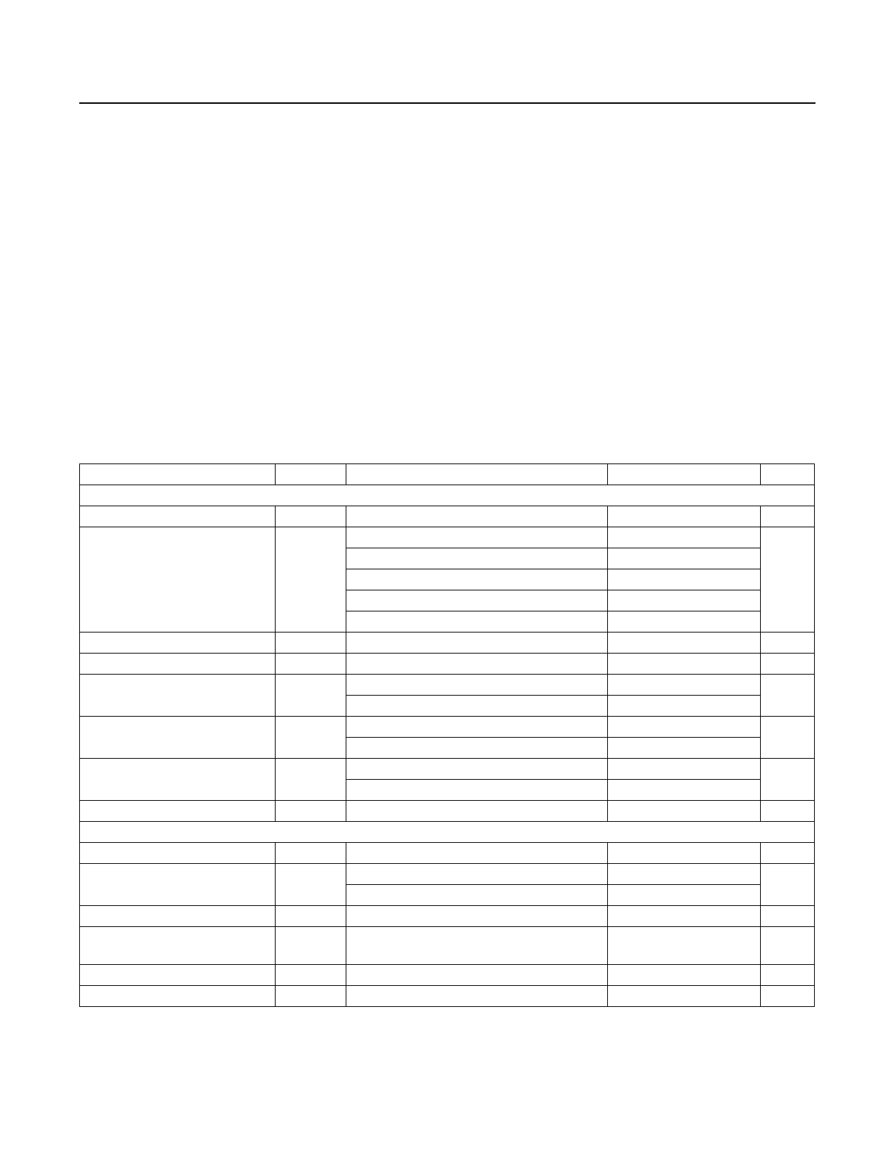
ELECTRICAL CHARACTERISTICS
(VCC = +3.0V to +5.5V, TA = -55°C to +125°C, unless otherwise noted. Typical values are VCC = +3.3V, TA = +25°C, unless other-
wise noted.)
PARAMETER
SYMBOL
CONDITIONS
TEMPERATURE-TO-DIGITAL CONVERTER CHARACTERISTICS
Supply Range
VCC
0°C ≤ TA = ≤ +50°C, VCC = +3.3V
MIN TYP MAX UNITS
3.0
5.5
V
-1.0 ±0.4 +1.0
-20°C ≤ TA = ≤ +85°C, VCC = +3.3V
-1.5 ±0.6 +1.5
Accuracy (Note 1)
-40°C ≤ TA = ≤ 125°C, VCC = +3.3V
-2.5 ±1.0 +2.5
°C
TA = -55°C, VCC = +3.3V
TA = +150°C, VCC = +3.3V
Power-Supply Rejection Ratio
PSRR
POR Threshold Hysteresis
Supply Current in Shutdown
Average Operating Current
Peak Operating Current (Note 2)
Conversion Rate
DIGITAL INTERFACE
Logic Input Low Voltage
Logic Input High
Voltage
Input Leakage Current
Output Low Sink Current
Output Leakage Current
Input Capacitance
VIL
VIH
II_LEAK
IOL
IO_LEAK
CIN
VCC = +3.0V, SMBus inactive
VCC = +5.5V, SMBus inactive
VCC = +3.0V, SMBus inactive
VCC = +5.5V, SMBus inactive
VCC = +3.0V, SMBus inactive
VCC = +5.5V, SMBus inactive
VCC = +3.0V to +5.5V
VCC = +3V
VCC = +5.5V
VIN = GND or VCC
VOL = 0.6V (SMBDATA,
ALERT, OVERT)
ALERT, OVERT at VCC
-2.8 ±1.5 +2.8
±2.5
0.2
0.5
°C/V
90
mV
12
20
µA
20
30
150
µA
200
270
350
µA
350
700
1.4
2
2.4
Hz
0.65
V
2.2
V
2.4
±1
µA
6
mA
±1
µA
5
pF
2 _______________________________________________________________________________________
Share Link: