MAX6819 데이터 시트보기 (PDF) - Maxim Integrated
부품명
상세내역
제조사
MAX6819 Datasheet PDF : 8 Pages
| |||
SOT23 Power-Supply Sequencers
PIN
MAX6819 MAX6820
1
1
2
2
3
3
4
—
—
4
5
5
6
6
Pin Description
NAME
VCC1
GND
SETV
EN
SETD
GATE
VCC2
FUNCTION
Supply Voltage 1. Either VCC1 or VCC2 must be greater than the UVLO to enable
external MOSFET drive.
Ground
Sequence Threshold Set. Connect to an external resistor-divider network to set the
VCC1 threshold that enables GATE turn-on. The internal reference is 0.618V.
Active-High Enable. GATE drive is enabled tDELAY after EN is driven high. GATE
drive is immediately disabled when EN is driven low. Connect to the higher of VCC1
and VCC2 if not used.
GATE Delay Set Input. Connect an external capacitor from SETD to GND to adjust
the delay from SETV > VTH to GATE turn-on. tDELAY (s) = 2.484 x 10⁶ x CSET (F).
GATE Drive Output. GATE drives an external n-channel MOSFET to connect VCC2 to
the load. GATE drive enables tDELAY after SETV exceeds VTH and ENABLE is driven
high. GATE drive is immediately disabled when SETV drops below VTH or ENABLE is
driven low. When enabled, an internal charge pump drives GATE to VCC2 + 5.5V to
fully enhance the external n-channel MOSFET.
Supply Voltage 2. Either VCC1 or VCC2 must be greater than the UVLO to enable
external MOSFET drive.
Detailed Description
Many dual-supply processors or multivoltage boards
require one power supply to rise to the proper operat-
ing voltage before another supply is applied. Improper
sequencing can lead to chip latchup, incorrect device
initiation, or long-term reliability degradation. If the vari-
ous supply voltages are not locally generated (coming
from a main system bus, an externally purchased silver
box, or a nonsequenced power management chip),
power-on and power-off sequencing can be difficult to
control or predict. Supply loading can affect turn-
on/turn-off times from board to board.
The MAX6819/MAX6820 provide proper local voltage
sequencing in multisupply systems. The sequencers use
an external n-channel MOSFET to switch the secondary
supply to the load only when the primary supply is above
a desired operating voltage threshold. The n-channel
MOSFET operates in a default off mode when the primary
supply is below the desired threshold or if neither supply
exceeds the sequencer’s UVLO level.
When the primary supply voltage is above the set
threshold, the external MOSFET is driven on. An inter-
nal charge pump fully enhances the external MOSFET
by providing a gate-to-source voltage (VGS) of +5.5V
(typ). The charge pump fully enhances the MOSFET to
yield a low drain-to-source impedance (RDS(ON)) for
reduced switch voltage drop. The MOSFET is never dri-
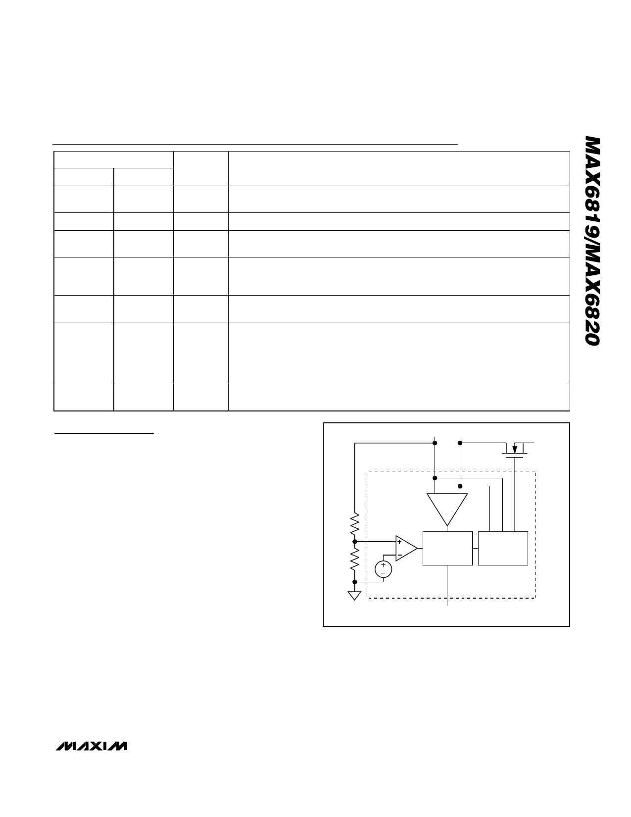
VCC1 VCC2
VCC2 OUT
GATE
UVLO
SETV
SEQUENCE
DELAY/
LOGIC
GATE DRIVE
CHARGE PUMP
0.62V
GND
( ) FOR MAX6820 ONLY
EN (SETD)
Figure 1. Functional Diagram
ven on unless the sequencer can provide a minimum
VGS enhancement, ensuring that the switch MOSFET
never operates in its higher impedance linear range.
Either supply may act as the primary source, regard-
less of the voltage level, provided that VCC1 or VCC2 is
greater than 2.125V (Figure 1 and Figure 2).
_______________________________________________________________________________________ 5
Share Link: 