MAX6819 데이터 시트보기 (PDF) - Maxim Integrated
부품명
상세내역
제조사
MAX6819 Datasheet PDF : 8 Pages
| |||
SOT23 Power-Supply Sequencers
Applications Information
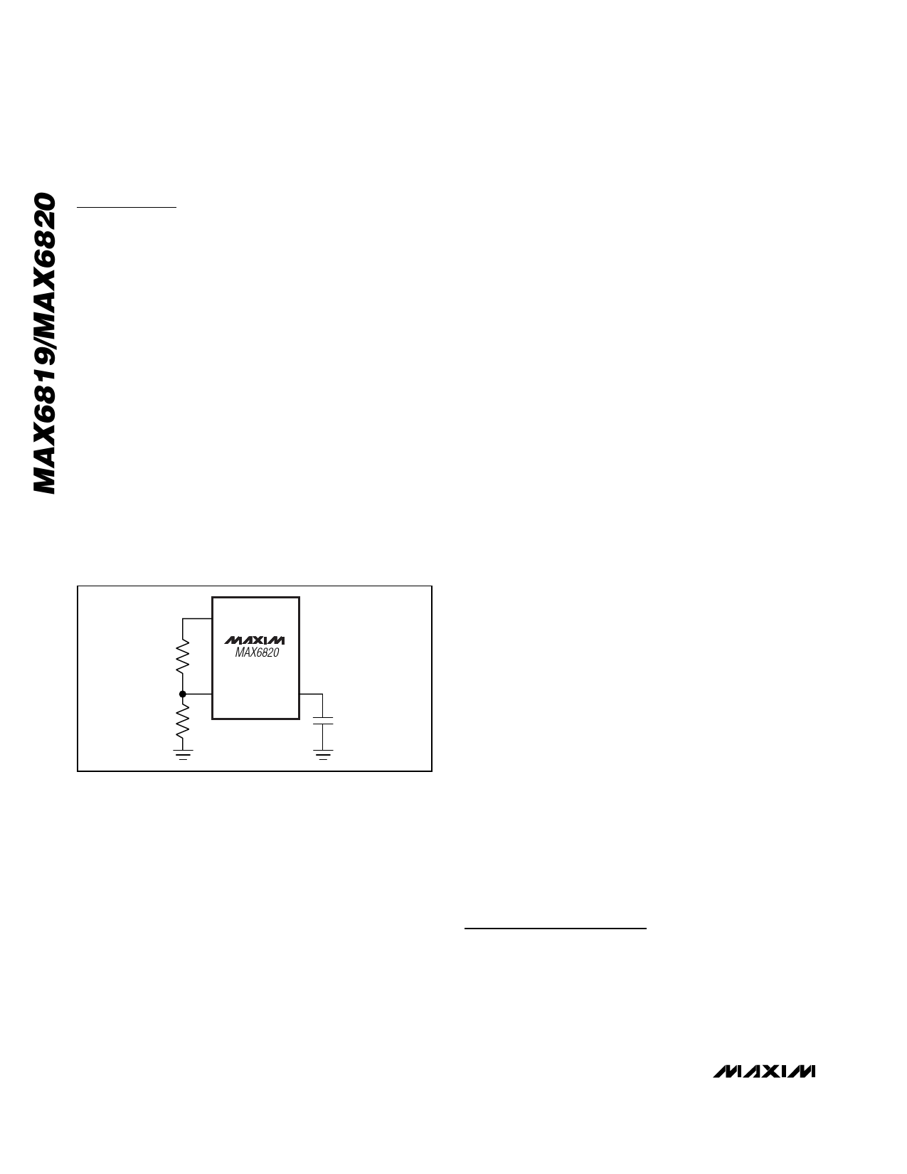
Adjusting tDELAY
The MAX6820 features a capacitor adjustable
sequence delay. The adjustable delay provides power
sequencing for a wide range of devices with different
power-supply delay requirements. Connect a capacitor
(CSET) between SETD and GND to adjust the delay
time (Figure 2). Calculate the sequence delay time as
follows:
tDELAY (s) = 2.48 ✕ 106 ✕ CSET
Setting Threshold Voltage at SETV
The threshold voltage is the minimum VCC1 voltage at
which VCC2 turn-on is acceptable. To monitor voltages
higher than the threshold voltage, connect external
resistors as a voltage-divider to SETV, and calculate the
minimum VCC turn-on voltage as follows:
R1 = R2 ((VTRIP / VTH) - 1)
where VTRIP is the minimum turn-on voltage at VCC1
and VTH = 0.618V (Figure 2).
Since SETV input current is 10nA (typ), high value resis-
tors can be used.
VCC1
R1
MAX6820
SETV
SETD
R2
CSET
Figure 2. tDELAY (MAX6820 ONLY) and VTH Adjust
Selecting the Pass MOSFET
The external pass MOSFET is connected in series with
the sequenced power-supply source. Since the load
current and the MOSFET drain-to-source impedance
(RDS) determine the voltage drop, the on characteristics
of the MOSFET affect the load supply accuracy. The
MAX6819/MAX6820 fully enhance the external MOSFET
out of its linear range to ensure the lowest drain-to-
source on impedance. For highest supply accuracy/
lowest voltage drop, select a MOSFET with an appropri-
ate drain-to-source on impedance for a gate-to-source
bias of 4.5V to 6.0V.
Gate Drive Characteristics
The MAX6819/MAX6820 internal charge pump drives
the n-channel MOSFET with a gate-to-source voltage
(VGS) of 5.5V, ensuring low MOSFET on-resistance
RDS(ON). The charge pump drives the high-impedance
capacitive load of a MOSFET gate input.
Loading the GATE output resistively adds load current
and reduces gate drive capability. The internal charge
pump does not require external capacitors.
The external pass MOSFET is disabled, and charge
pump circuitry is turned off when neither VCC1 nor VCC2
are above the 1.875V UVLO or EN is low.
Logic Driven Supply Sequencing
The MAX6819 offers a logic-compatible enable input
(EN) that allows digital devices to control sequencing.
When the TTL/CMOS-compatible EN input is logic-low,
the GATE output is low. When the EN input is logic-high
(and SETV is above the monitor threshold), the GATE
output is enabled after an internally fixed 200ms delay.
For a logic-controlled sequencer when voltage monitor-
ing is not desired, connect SETV to VCC1 or VCC2 >
0.62V (Figure 3).
Sequencing Three or More Supplies
Cascade multiple MAX6819/MAX6820 to sequence
more than two supplies. Daisy-chaining devices allows
one sequencer to monitor the passed voltage of an
upstream sequencer through the SETV comparator
inputs. EN allows any sequencer to be shut down inde-
pendent of the SETV levels. Figure 4 shows an example
of a three-supply system in which the first supply must
come up before the second supply and the third supply
must yield for both supplies.
Negative-Going Voltage
Transient Immunity
The MAX6819/MAX6820 power-supply voltage sequen-
cers are relatively immune to short-duration (pulse
width), negative-going voltage transients (Figure 5).
However, the amplitude of the transient is inversely pro-
portional to its pulse width.
Chip Information
TRANSISTOR COUNT: 638
PROCESS: BiCMOS
6 _______________________________________________________________________________________
Share Link: 