MAX767RCAP 데이터 시트보기 (PDF) - Maxim Integrated
부품명
상세내역
제조사
MAX767RCAP Datasheet PDF : 19 Pages
| |||
5V-to-3.3V, Synchronous, Step-Down
Power-Supply Controller
VCC MAX767
PWM
LEVEL
TRANSLATOR
BST
DH
LX
VCC
DL
VIN
C1
D1
C3
N1
L1
N2
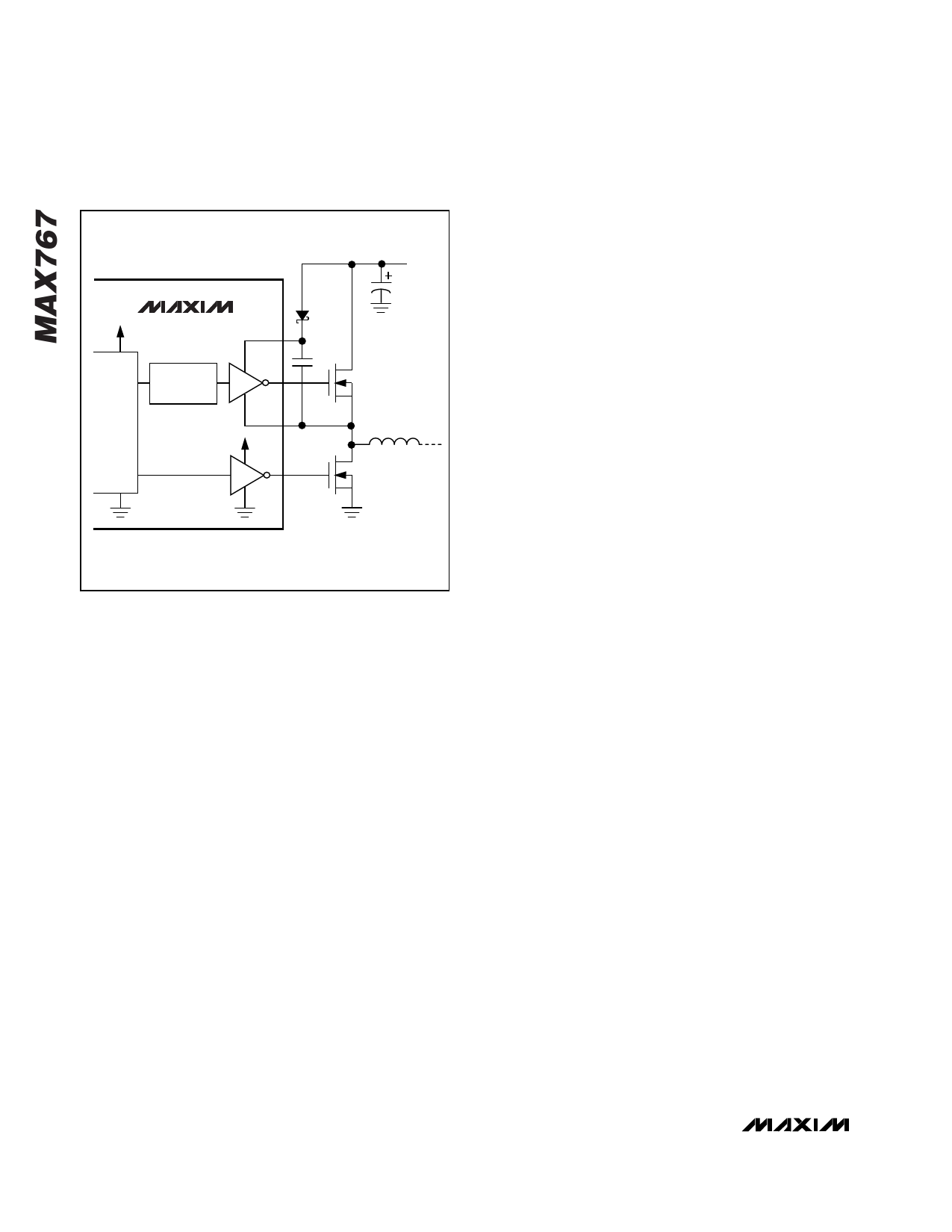
Figure 4. Boost Supply for High-Side Gate Driver
Gate-Driver Boost Supply
Gate-drive voltage for the high-side N-channel switch is
generated with the flying-capacitor boost circuit shown
in Figure 4. The capacitor (C3) is alternately charged
from the 5V input via the diode (D1) and placed in par-
allel with the high-side MOSFET’s gate-source termi-
nals. On start-up, the synchronous rectifier (low-side)
MOSFET (N2) forces LX to 0V and charges the BST
capacitor to 5V. On the second half-cycle, the PWM
turns on the high-side MOSFET (N1); it does this by
closing an internal switch between BST and DH, which
connects the capacitor to the MOSFET gate. This pro-
vides the necessary enhancement voltage to turn on
the high-side switch, an action that “boosts” the 5V
gate-drive signal above the input voltage.
Ringing seen at the high-side MOSFET gates (DH) in
discontinuous-conduction mode (light loads) is a natur-
al operating condition. It is caused by the residual
energy in the tank circuit, formed by the inductor and
stray capacitance at the LX node. The gate-driver neg-
ative rail is referred to LX, so any ringing there is direct-
ly coupled to the gate-drive supply.
Modes of Operation
PWM Mode
Under heavy loads—over approximately 25% of full
load—the supply operates as a continuous-current
PWM supply (see Typical Operating Characteristics).
The duty cycle, %ON, is approximately:
%ON = __V_O_U_T___
VIN
Current flows continuously in the inductor: first, it ramps
up when the power MOSFET conducts; second, it
ramps down during the flyback portion of each cycle as
energy is put into the inductor and then discharged into
the load. Note that the current flowing into the inductor
when it is being charged is also flowing into the load,
so the load is continuously receiving current from the
inductor. This minimizes output ripple and maximizes
inductor use, allowing very small physical and electrical
sizes. Output ripple is primarily a function of the filter
capacitor’s effective series resistance (ESR), and is
typically under 50mV (see Design Procedure section).
Idle-Mode
Under light loads (<25% of full load), the MAX767
enhances efficiency by turning the drive voltage on and
off for only a single clock period, skipping most of the
clock pulses entirely. Asynchronous switching, seen as
“ghosting” on an oscilloscope, is thus a normal operat-
ing condition whenever the load current is less than
approximately 25% of full load.
At certain input voltage and load conditions, a transition
region exists where the controller can pass back and
forth from idle-mode to PWM mode. In this situation,
short pulse bursts occur, which make the current wave-
form look erratic but do not materially affect the output
ripple. Efficiency remains high.
Current Limiting
The voltage between CS and FB is continuously moni-
tored. An external, low-value shunt resistor is connect-
ed between these pins, in series with the inductor,
allowing the inductor current to be continuously mea-
sured throughout the switching cycle. Whenever this
voltage exceeds 100mV, the drive voltage to the exter-
nal high-side MOSFET is cut off. This protects the MOS-
FET, the load, and the input supply in case of short cir-
cuits or temporary load surges. The current-limiting
resistance is typically 20mΩ for 3A.
10 ______________________________________________________________________________________
Share Link: 