MAX9680 데이터 시트보기 (PDF) - Maxim Integrated
부품명
상세내역
제조사
MAX9680 Datasheet PDF : 9 Pages
| |||
3V Video Amplifier with
Internal Gain and Filter in SC70
ABSOLUTE MAXIMUM RATINGS
Supply Voltage (VDD to GND).................................-0.3V to +4V
ENABLE to GND......................................................-0.3V to +4V
IN to GND................................................. -0.3V to (VDD + 0.3V)
OUT to GND (ENABLE is high)................ -0.3V to (VDD + 0.3V)
OUT to GND (ENABLE is low)..............................-0.3V to +3.2V
ENABLE, IN...................................................................... Q50mA
OUT............................................................................ Continuous
Electrostatic Discharge
Human Body Model.......................................................2000V
Charged Device Model....................................................500V
Continuous Power Dissipation (TA = +70NC)
6-Pin SC70 (derate 3.1mW/C above +70NC)..............245mW
Operating Temperature Range......................... -40NC to +125NC
Junction Temperature......................................................+150NC
Storage Temperature Range............................ -65NC to +150NC
Lead Temperature (soldering, 10s).................................+300NC
Soldering Temperature (reflow).......................................+260NC
PACKAGE THERMAL CHARACTERISTICS (Note 1)
SC70
Junction-to-Ambient Thermal Resistance (qJA)......326.5°C/W
Junction-to-Case Thermal Resistance (qJC)..............115°C/W
Note 1: Package thermal resistances were obtained using the method described in JEDEC specification JESD51-7, using a 4-layer
board. For detailed information on package thermal considerations, refer to www.maxim-ic.com/thermal-tutorial.
Stresses beyond those listed under “Absolute Maximum Ratings” may cause permanent damage to the device. These are stress ratings only, and functional
operation of the device at these or any other conditions beyond those indicated in the operational sections of the specifications is not implied. Exposure to absolute
maximum rating conditions for extended periods may affect device reliability.
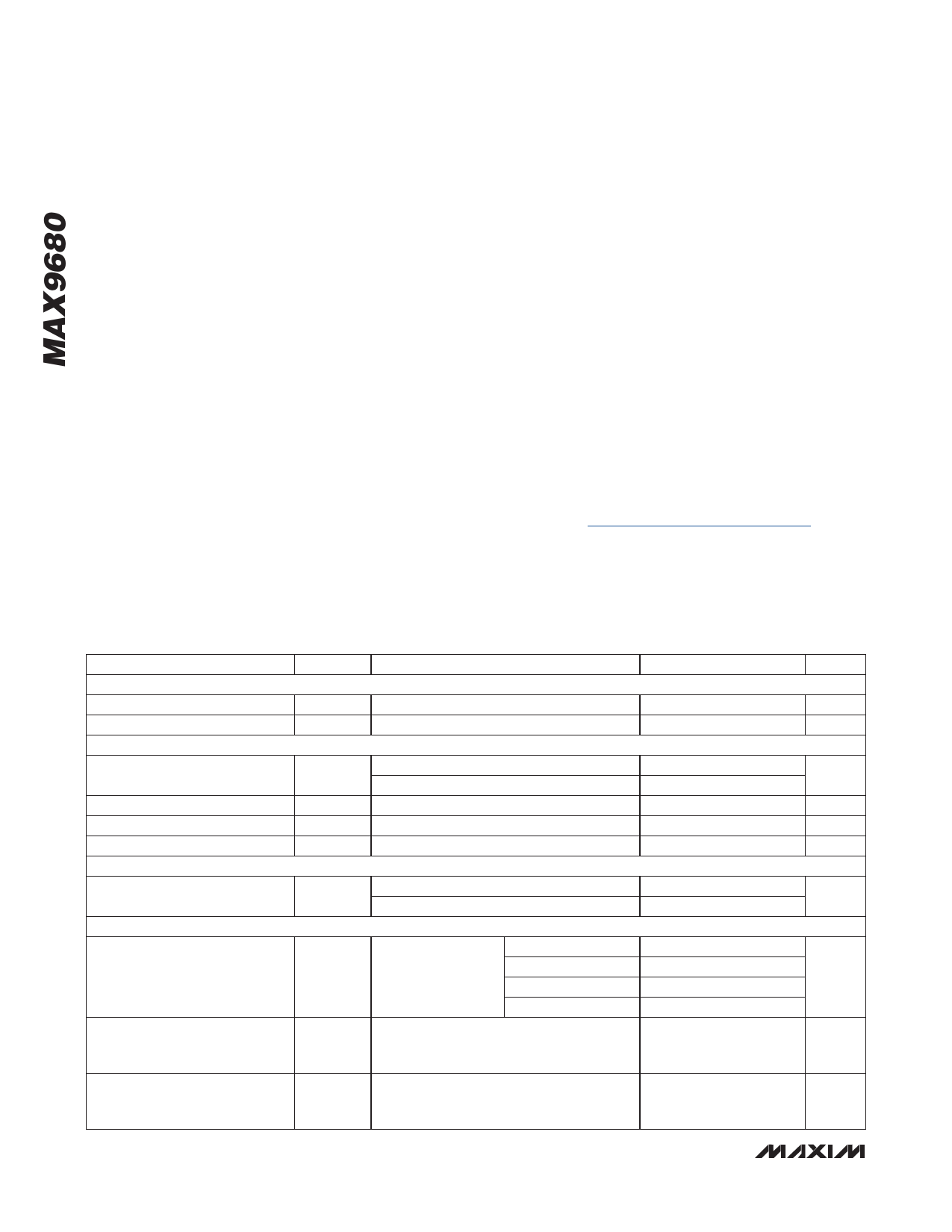
ELECTRICAL CHARACTERISTICS
(VDD = VENABLE = 2.8V, VGND = 0V, RL = 150I to GND. TA = -40NC to +125NC, unless otherwise noted. Typical values are at TA
= +25NC.) (Note 2)
PARAMETER
SYMBOL
CONDITIONS
OFFSET LEVEL-SHIFT VOLTAGE
Output Level-Shift Voltage
Power-Supply Rejection Ratio
INPUT VOLTAGE RANGE
VOLS
PSRR
VIN = VGND
VIN = VGND, VDD = 2.7V to 3.6V
Input Voltage Range
Input Resistance (In+)
RSET Resistance
RSET/RIN Ratio
VOLTAGE GAIN
VCM
RIN
RSET
VDD = 2.7V
VDD = 2.8V
VIN = 0.5V
VRSET = 0.5V
DC Voltage Gain (Note 3)
FREQUENCY RESPONSE
AV
VDD = 2.7V, VIN = VGND to 0.445V
VDD = 2.8V, VIN = VGND to 0.464V
f = 4.5MHz
Filter Response
VIN = VGND to
0.387V
f = 9MHz
f = 27MHz
f = 54MHz
Differential Gain Error
Five-step modulated staircase of 127.8mV
step size and 305.3mV peak-to-peak
subcarrier amplitude, f = 4.43MHz
MIN TYP MAX UNITS
0
120 250
mV
200
FV/V
VGND
VGND
0.445
V
0.464
732 872 1012
I
3150 3750 4350
I
4.214 4.3 4.386
5.00 5.17 5.34
V/V
5.00 5.17 5.34
-0.2
-3.5
dB
-23
-45
0.2
%
Differential Phase Error
Five-step modulated staircase of 127.8mV
step size and 305.3mV peak-to-peak
subcarrier amplitude, f = 4.43MHz
0.3
degrees
2 _______________________________________________________________________________________
Share Link: 