MPC5534MZQ40R2 데이터 시트보기 (PDF) - Freescale Semiconductor
부품명
상세내역
제조사
MPC5534MZQ40R2 Datasheet PDF : 50 Pages
| |||
Electrical Characteristics
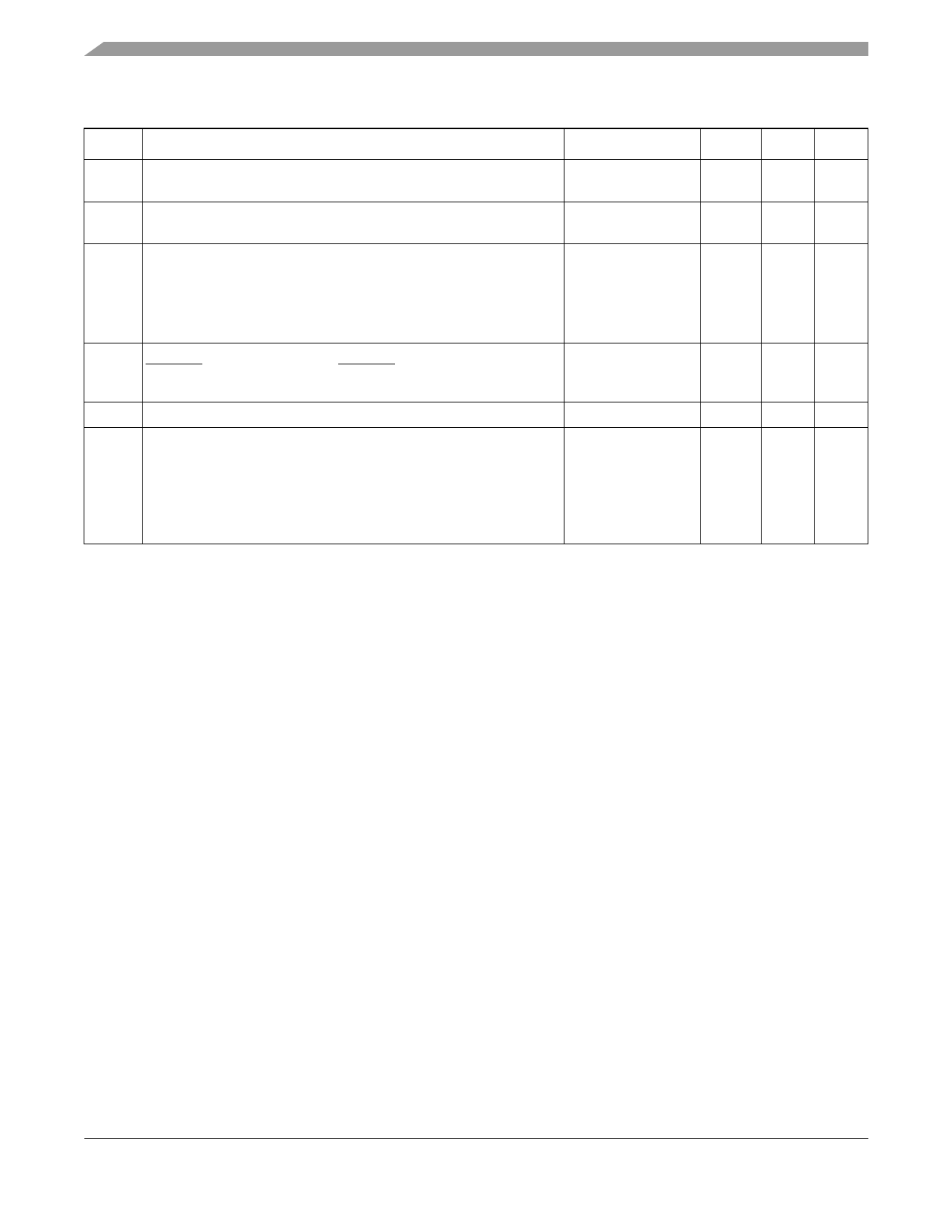
Table 6. VRC/POR Electrical Specifications (continued)
Num
Characteristic
Symbol
Min Max Units
5 VRC33 voltage when regulator controller allows the pass transistor V_TRANS_ON
to completely turn on1, 2
2.0 2.85 V
6 VRC33 voltage above which the regulator controller will keep the
V_VRC33REG
3.0
—
V
1.5V supply in regulation3, 4
7 Current which can be sourced by VRCCTL
I_VRCCTL5
mA
– 40C
11.0
—
mA
25C
9.0
— mA
150C (Tj)
7.5
— mA
8 Voltage differential during power up that VDD33 can lag VDDSYN or
VDDEH6 before VDDSYN and VDDEH6 reach V_POR33 and
V_POR5 minimums respectively
VDD33_LAG
—
1.0
V
9 Absolute value of Slew Rate on power supply pins
—
50 V/ms
10 Required Gain:
Idd / I_VRCCTL (@vdd = 1.35v, fsys = 80MHz)4, 6
– 40C
BETA7
35.08
—
—
25C
40.08
—
—
150C (Tj)
50.08 500
—
1 User must be able to supply full operating current for the 1.5V supply when the 3.3V supply reaches this range.
2 Current limit may be reached during ramp up and should not be treated as short circuit current.
3 At peak current for device.
4 Assumes that the Freescale recommended board requirements and transistor recommendations are met. Board signal
traces/routing from the VRCCTL package signal to the base of the external pass transistor and between the emitter of the pass
transistor to the VDD package signals should have a maximum of 100 nH inductance and minimal resistance (<1 ohm).
VRCCTL should have a nominal 1µF phase compensation capacitor to ground. VDD should have a 20 µF (nominal) bulk
capacitor (> 4 µF over all conditions, including lifetime). High frequency bypass capacitors consisting of eight 0.01 µF, two 0.1
µF, and one 1 µF capacitors should be place around the package on the VDD supply signals.
5 I_VRCCTL measured at the following conditions: VDD=1.35V, VRC33=3.1V, V_VRCCTL=2.2V.
6 Values are based on IDD from high use applications as explained in the IDD Electrical Specification.
7 BETA is measured on a per part basis and is calculated as IDD / I_VRCCTL and represents the worst case external transistor
BETA.
8 Preliminary value. Final specification pending characterization.
3.7 Power Up/Down Sequencing
Power sequencing between the 1.5-V power supply and VDDSYN or the RESET power supplies is
required if the user provides an external 1.5-V power supply and ties VRC33 to ground. To avoid this
power sequencing requirement, power up VRC33 within the specified operating range, even if not using
the on-chip voltage regulator controller. Refer to Section 3.7.1, “Power Up Sequence (If VRC33
Grounded)” and Section 3.7.2, “Power Down Sequence (If VRC33 Grounded).”
Another power sequencing requirement is that VDD33 must be of sufficient voltage before POR negates,
so that the values on certain pins are treated as 1s when POR does negate. Refer to Section 3.7.3, “Input
Value of Pins During POR Dependent on VDD33.”
MPC5534 Microcontroller Data Sheet, Rev. 0
10
Preliminary—Subject to Change Without Notice
Freescale Semiconductor
Share Link: 