74LVCH16541A 데이터 시트보기 (PDF) - Philips Electronics
부품명
상세내역
제조사
74LVCH16541A Datasheet PDF : 10 Pages
| |||
Philips Semiconductors
16-bit buffer/line driver; 5V tolerant I/O (3-State)
Product specification
74LVCH16541A
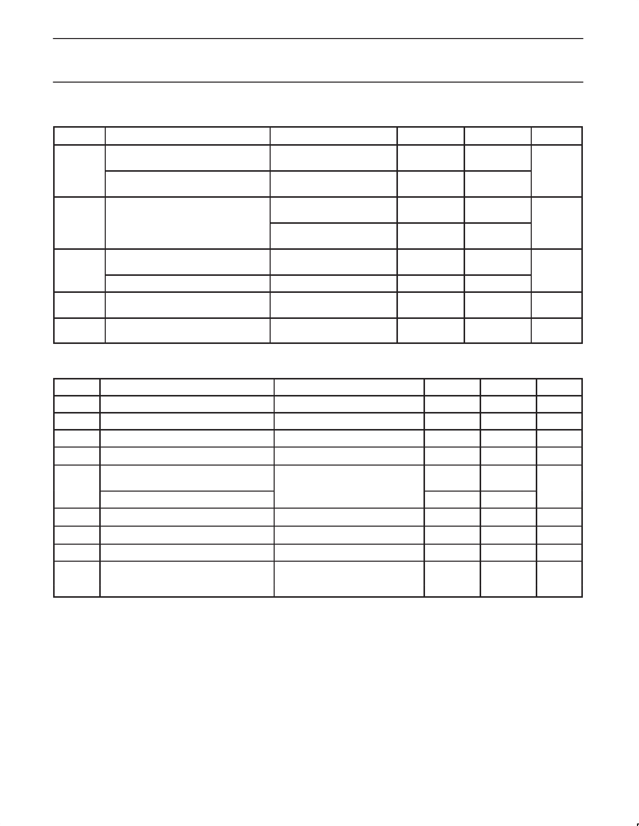
RECOMMENDED OPERATING CONDITIONS
SYMBOL
PARAMETER
CONDITIONS
DC supply voltage
(for maximum speed performance)
VCC
DC supply voltage
(for low-voltage applications)
VI
DC Input voltage range
For data input pins with
bus hold
For data input pins without
bus hold
DC output voltage range;
VO
output HIGH or LOW state
DC output voltage range; output 3-State
Tamb
Operating ambient temperature range
in free air
tr, tf
Input rise and fall times
VCC = 1.2 to 2.7V
VCC = 2.7 to 3.6V
MIN.
2.7
1.2
0
0
0
0
–40
0
0
MAX.
3.6
3.6
VCC
5.5
VCC
5.5
+85
20
10
UNIT
V
V
V
°C
ns/V
ABSOLUTE MAXIMUM VALUES1, 2
In accordance with the Absolute Maximum Rating System (IEC 134) Voltages are referenced to GND (ground = 0V)
SYMBOL
PARAMETER
CONDITIONS
MIN
MAX
UNIT
VCC DC supply voltage
IIK
DC input diode current
VI
DC input voltage
IOK
DC output diode current
DC output voltage; output HIGH or LOW
VO
state
DC output voltage; output 3-State
VI < 0
Note 3
VO > VCC or VO < 0
Note 3
–0.5
+6.5
V
–
–50
mA
–0.5
+6.5
V
–
"50
mA
–0.5
VCC + 0.5
V
–0.5
6.5
IO
DC output source or sink current
VO = 0 to VCC
–
"50
mA
IGND, ICC DC VCC or GND current
–
"100
mA
Tstg
Storage temperature range
–65
+150
°C
Power dissipation per package
For temperature range: –40 to +125°C
Ptot
– SSOP (plastic medium-shrink)
– TSSOP (plastic thin-medium-shrink)
above +70°C derate linearly 8mW/K
above +60°C derate linearly 5.5mW/K
500
mW
500
NOTES:
1. Stresses beyond those listed may cause permanent damage to the device. These are stress ratings only and functional operation of the
device at these or any other conditions beyond those indicated under “recommended operating conditions” is not implied. Exposure to
absolute-maximum-rated conditions for extended periods may affect device reliability.
2. The performance capability of a high-performance integrated circuit in conjunction with its thermal environment can create junction
temperatures which are detrimental to reliability. The maximum junction temperature of this integrated circuit should not exceed 150°C.
3. The input and output voltage ratings may be exceeded if the input and output clamp current ratings are observed.
1998 May 19
4
Share Link: 