NX25P10 데이터 시트보기 (PDF) - Unspecified
부품명
상세내역
제조사
NX25P10 Datasheet PDF : 28 Pages
| |||
1M / 2M / 4M-BIT SERIAL FLASH MEMORY with 40MHz SPI
NX25P10, NX25P20 AND NX25P40
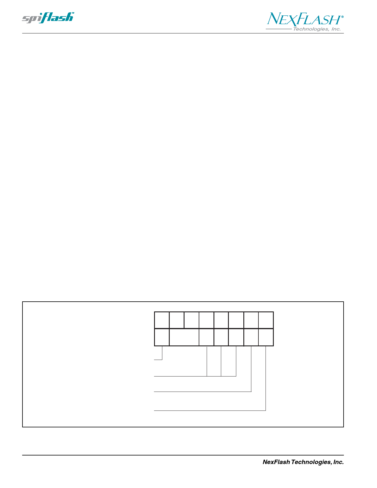
STATUS REGISTER
The Read Status Register instruction can be used to provide
status on the availability of the Flash memory array, if the
device is write enabled or disabled, and the state of write
protection. The Write Status Register instruction can be
used to configure the devices write protection features. See
Figure 3.
BUSY
BUSY is a read only bit in the status register (S0) that is set
to a 1 state when the device is executing a Page Program,
Sector Erase, Bulk Erase or Write Status Register instruc-
tion. During this time the device will ignore further instruc-
tions except for the Read Status Register instruction (see
tW, tPP, tSE and tBE in AC Characteristics). When the
program, erase or write status register instruction has
completed, the BUSY bit will be cleared to a 0 state
indicating the device is ready for further instructions.
Write Enable Latch (WEL)
Write Enable Latch (WEL) is a read only bit in the status
register (S1) that is set to a 1 after executing a Write Enable
Instruction. The WEL status bit is cleared to a 0 when the
device is write disabled. A write disable state occurs upon
power-up or after any of the following instructions: Write
Disable, Page Program, Sector Erase, Bulk Erase and
Write Status Register.
Block Protect Bits (BP2, BP1, BP0)
The Block Protect Bits (BP2, BP1, BP0) are non-volatile
read/write bits in the status register (S4, S3, S2) that provide
Write Protection control and status. Block Protect bits can
be set using the Write Status Register Instruction (see tW
in AC characteristics). All, none or a portion of the memory
array can be protected from Program and Erase instructions
(see table 2). The factory default setting for the Block
Protection Bits is 0, none of the array protected. The Block
Protect bits can not be written to if the Status Register
Protect (SRP) bit is set to 1 and the Write Protect (WP) pin
is low. The NX25P20 and NX25P10 do not use BP2.
Reserved Bits
Status register bit locations 5 and 6 are reserved for future
use. Current devices will read 0 for these bit locations. It is
recommended to mask out the reserved bit when testing the
Status Register. Doing this will ensure compatibility with
future devices.
Status Register Protect (SRP)
The Status Register Protect (SRP) bit is a non-volatile read/
write bit in the status register (S7) that can be used in
conjunction with the Write Protect (WP) pin to disable writes
to the status register. When the SRP bit is set to a 0 state
(factory default) the WP pin has no control over the status
register. When the SRP pin is set to a 1, the Write Status
Register instruction is locked out while the WP pin is low.
When the WP pin is high the Write Status Register instruc-
tion is allowed.
S7 S6 S5 S4 S3 S2 S1 S0
SRP (Reserved) BP2 BP1 BP0 WEL BUSY
Status RegisterProtect
(Non-volatile)
Block Protect Bits
(Non-volatile)
Write Enable Latch
Device Busy
Erase Program or Write in Progress
Figure 3. Status Register Bit Locations
8
NexFlash Technologies, Inc.
PRELIMINARY MKP-0009 Rev 6 NXSF040I-0405
04/04/05 ©
Share Link: 