OR4E10 데이터 시트보기 (PDF) - Agere -> LSI Corporation
부품명
상세내역
제조사
OR4E10 Datasheet PDF : 124 Pages
| |||
Preliminary Data Sheet
December 2000
Product Description (continued)
EMBEDDED
MICROPROCESSOR
INTERFACE (MPI)
EMBEDDED
BLOCK RAM
ORCA Series 4 FPGAs
HIGH-SPEED I/Os
SYSTEM BUS
PFU
SLIC
PLC
FPGA/SYSTEM
BUS INTERFACE
CLOCK PINS
PIO
PLLs
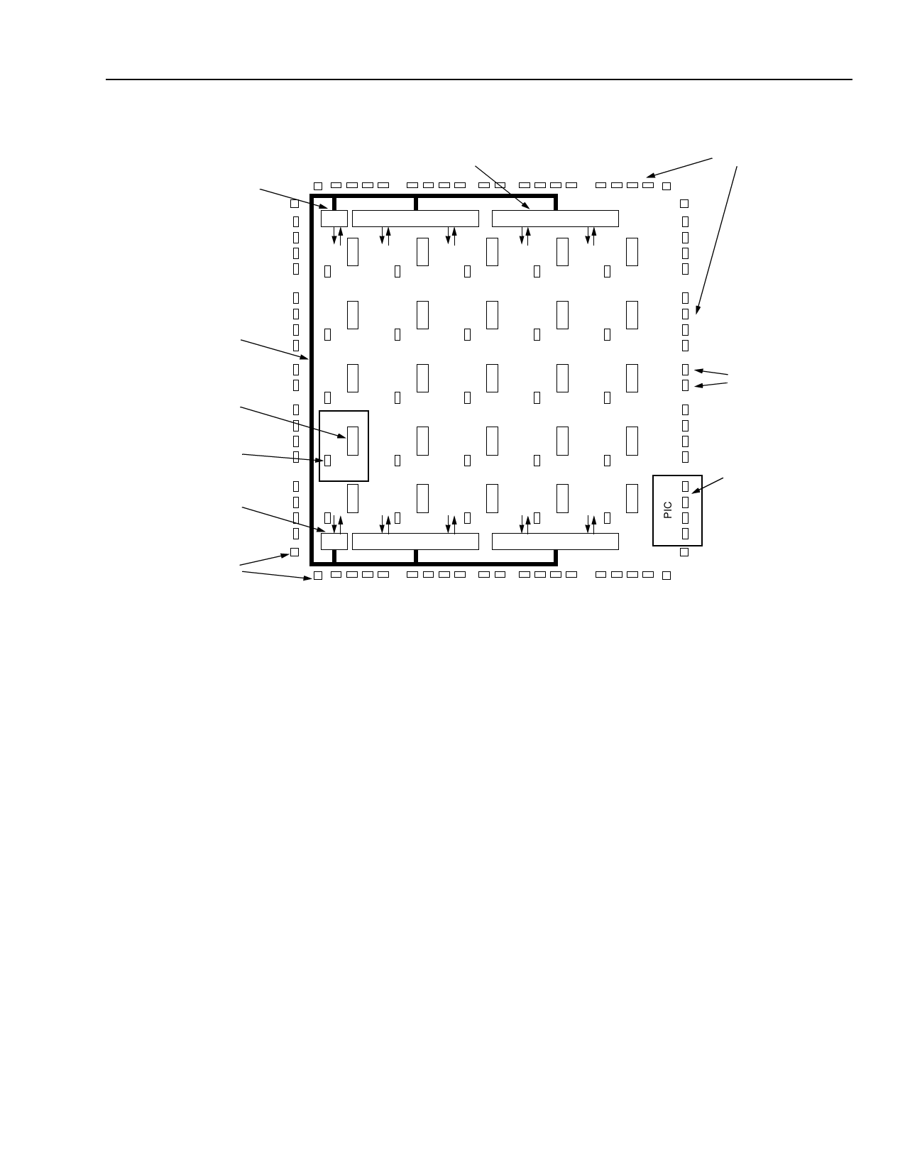
Figure 1. Series 4 Top-Level Diagram
5-7536 (F)a
Programmable Logic Cells
The PLCs are arranged in an array of rows and col-
umns. The location of a PLC is indicated by its row and
column so that a PLC in the second row and the third
column is R2C3. The array of actual PLCs for every
device begins with R3C2 in all Series 4 generic
FPGAs.
The PLC consists of a PFU, SLIC, and routing
resources. Each PFU within a PLC contains eight
4-input (16-bit) LUTs, eight latches/FFs, and one addi-
tional FF that may be used independently or with arith-
metic functions. The PFU is the main logic element of
the PLC, containing elements for both combinatorial
and sequential logic. Combinatorial logic is done in
LUTs located in the PFU. The PFU can be used in dif-
ferent modes to meet different logic requirements. The
LUTs twin-quad architecture provides a configurable
medium-/large-grain architecture that can be used to
implement from one to eight independent combinatorial
logic functions or a large number of complex logic func-
tions using multiple LUTs. The flexibility of the LUT to
handle wide input functions, as well as multiple smaller
input functions, maximizes the gate count per PFU
while increasing system speed.
Lucent Technologies Inc.
7
Share Link: 