M80C186EB-8 데이터 시트보기 (PDF) - Intel
부품명
상세내역
제조사
M80C186EB-8 Datasheet PDF : 56 Pages
| |||
M80C186EB
BUS INTERFACE UNIT
The M80C186EB core incorporates a bus controller
that generates local bus control signals In addition
it employs a HOLD HLDA protocol to share the local
bus with other bus masters
The bus controller is responsible for generating 20
bits of address read and write strobes bus cycle
status information and data (for write operations) in-
formation It is also responsible for reading data off
the local bus during a read operation A READY in-
put pin is provided to extend a bus cycle beyond the
minimum four states (clocks)
A HOLD HLDA protocol is provided by the local bus
controller to allow multiple bus masters to share the
same local bus When the M80C186EB relinquishes
control of the local bus it floats certain bus control
signals to allow another bus master to drive these
pins directly Refer to the Pin Description section to
determine which pins the M80C186EB will float dur-
ing a HOLD HLDA bus exchange
The M80C186EB local bus controller also generates
two control signals (DEN and DT R) when interfac-
ing to external transceiver chips This capability al-
lows the addition of transceivers for simple buffering
of the mulitplexed address data bus
CLOCK GENERATOR
The M80C186EB provides an on-chip clock genera-
tor for both internal and external clock generation
The clock generator features a crystal oscillator a
divide-by-two counter and two low-power operating
modes
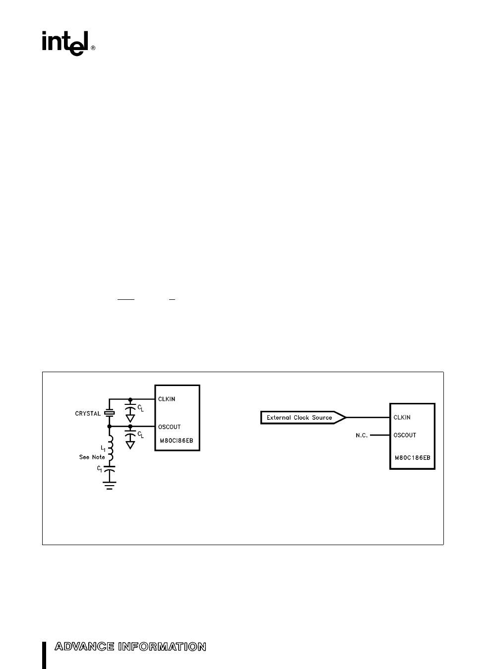
The oscillator circuit is designed to be used with ei-
ther a parallel resonant fundamental or third-over-
tone mode crystal network Alternatively the oscilla-
tor circuit may be driven from an external clock
source Figure 5 shows the various operating modes
of the M80C186EB oscillator circuit
The crystal or clock frequency chosen must be twice
the required processor operating frequency due to
the internal divide-by-two counter This counter is
used to drive all internal phase clocks and the exter-
nal CLKOUT signal CLKOUT is a 50% duty cycle
processor clock and can be used to drive other sys-
tem components All AC timings are referenced to
CLKOUT
The following parameters are recommended when
choosing a crystal
Temperature Range
Application Specific
ESR (Equivalent Series Resistance)
40X max
C0 (Shunt Capacitance of Crystal)
7 0 pF max
CL (Load Capacitance)
Drive Level
20 pF g 2 pF
1 mW max
271214 – 5
271214 –4
(A) Crystal Connection
(B) Clock Connection
NOTE
The L1C1 network is only required when using a third-
overtone crystal
Figure 5 M80C186EB Clock Configurations
9
Share Link: 