SC28L194 데이터 시트보기 (PDF) - Philips Electronics
부품명
상세내역
제조사
SC28L194 Datasheet PDF : 52 Pages
| |||
Philips Semiconductors
Quad UART for 3.3V and 5V supply voltage
Preliminary specification
SC28L194
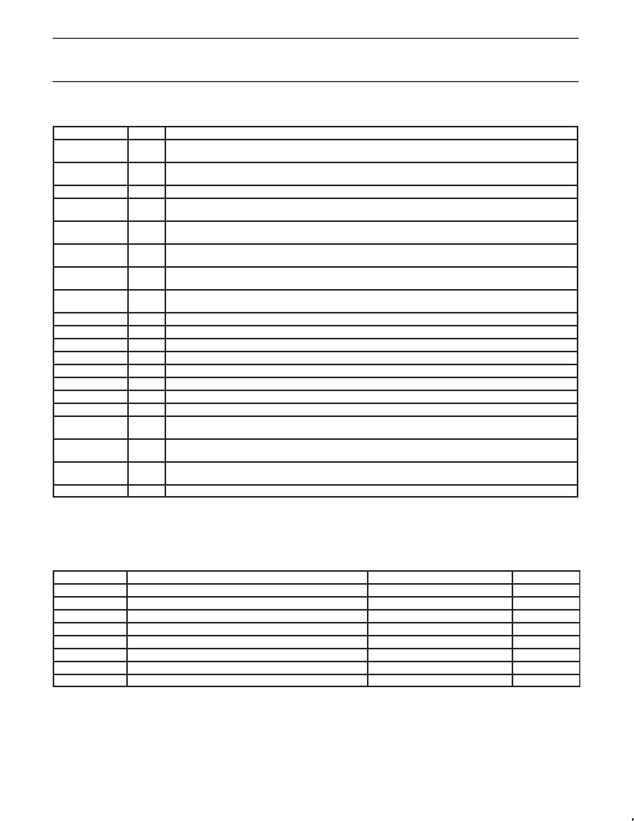
Pin Description
ÁÁÁÁÁÁÁÁÁÁÁÁÁÁÁÁÁÁÁÁÁÁÁÁÁÁÁÁÁÁÁÁÁÁ MNEMONIC
TYPE
ÁÁÁÁÁÁÁÁÁÁÁÁÁÁÁÁÁÁÁÁÁÁÁÁÁÁÁÁÁÁÁÁÁÁ SClk
I
ÁÁÁÁÁÁÁÁÁÁÁÁÁÁÁÁÁÁÁÁÁÁÁÁÁÁÁÁÁÁÁÁÁÁ CEN
I
ÁÁÁÁÁÁÁÁÁÁÁÁÁÁÁÁÁÁÁÁÁÁÁÁÁÁÁÁÁÁÁÁÁÁÁÁÁÁÁÁÁÁÁÁÁÁÁÁÁÁÁÁÁÁÁÁÁÁÁÁÁÁÁÁÁÁÁÁ A(7:0)
I
ÁÁÁÁÁÁÁÁÁÁÁÁÁÁÁÁÁÁÁÁÁÁÁÁÁÁÁÁÁÁÁÁÁÁ D(7:0)
I/O
ÁÁÁÁÁÁÁÁÁÁÁÁÁÁÁÁÁÁÁÁÁÁÁÁÁÁÁÁÁÁÁÁÁÁ W_RN
I
ÁÁÁÁÁÁÁÁÁÁÁÁÁÁÁÁÁÁÁÁÁÁÁÁÁÁÁÁÁÁÁÁÁÁ DACKN
O
ÁÁÁÁÁÁÁÁÁÁÁÁÁÁÁÁÁÁÁÁÁÁÁÁÁÁÁÁÁÁÁÁÁÁÁÁÁÁÁÁÁÁÁÁÁÁÁÁÁÁÁÁÁÁÁÁÁÁÁÁÁÁÁÁÁÁÁÁ IRQN
O
ÁÁÁÁÁÁÁÁÁÁÁÁÁÁÁÁÁÁÁÁÁÁÁÁÁÁÁÁÁÁÁÁÁÁ IACKN
I
ÁÁÁÁÁÁÁÁÁÁÁÁÁÁÁÁÁÁÁÁÁÁÁÁÁÁÁÁÁÁÁÁÁÁÁÁÁÁÁÁÁÁÁÁÁÁÁÁÁÁÁÁÁÁÁÁÁÁÁÁÁÁÁÁÁÁÁÁ TD(a-d)
O
ÁÁÁÁÁÁÁÁÁÁÁÁÁÁÁÁÁÁÁÁÁÁÁÁÁÁÁÁÁÁÁÁÁÁ RD(a-d)
I
I/O0(a-d)
I/O
ÁÁÁÁÁÁÁÁÁÁÁÁÁÁÁÁÁÁÁÁÁÁÁÁÁÁÁÁÁÁÁÁÁÁ I/O1(a-d)
I/O
ÁÁÁÁÁÁÁÁÁÁÁÁÁÁÁÁÁÁÁÁÁÁÁÁÁÁÁÁÁÁÁÁÁÁ I/O2(a-d)
I/O
ÁÁÁÁÁÁÁÁÁÁÁÁÁÁÁÁÁÁÁÁÁÁÁÁÁÁÁÁÁÁÁÁÁÁ I/O3(a-d)
I/O
ÁÁÁÁÁÁÁÁÁÁÁÁÁÁÁÁÁÁÁÁÁÁÁÁÁÁÁÁÁÁÁÁÁÁ Gin(1:0)
I
Gout(1:0)
O
ÁÁÁÁÁÁÁÁÁÁÁÁÁÁÁÁÁÁÁÁÁÁÁÁÁÁÁÁÁÁÁÁÁÁ RESETN
I
ÁÁÁÁÁÁÁÁÁÁÁÁÁÁÁÁÁÁÁÁÁÁÁÁÁÁÁÁÁÁÁÁÁÁÁÁÁÁÁÁÁÁÁÁÁÁÁÁÁÁÁÁÁÁÁÁÁÁÁÁÁÁÁÁÁÁÁÁ X1/CCLK
I
ÁÁÁÁÁÁÁÁÁÁÁÁÁÁÁÁÁÁÁÁÁÁÁÁÁÁÁÁÁÁÁÁÁÁ X2
O
ÁÁÁÁÁÁÁÁÁÁÁÁÁÁÁÁÁÁÁÁÁÁÁÁÁÁÁÁÁÁÁÁÁÁÁÁÁÁÁÁÁÁÁÁÁÁÁÁÁÁÁÁÁÁÁÁÁÁÁÁÁÁÁÁÁÁÁÁ Power Supplies
I
ÁÁÁÁÁÁÁÁÁÁÁÁÁÁÁÁÁÁÁÁÁÁÁÁÁÁÁÁÁÁÁÁÁÁ NOTE:
DESCRIPTION
Host system clock. Used to time operations in the Host Interface and clock internal logic. Must be greater than
twice the frequency of highest X1, Counter/Timer, TxC (1x) or RxC (1x) input frequency.
Chip select: Active low. When asserted, allows I/O access to QUART registers by host CPU. W_RN signal
indicates direction. (Must not be active in IACKN cycle)
Address lines (A[6] is NOT used. See “Host Interface” )
8-bit bi-directional data bus. Carries command and status information between 28L194 and the host CPU.
Used to convey parallel data for serial I/O between the host CPU and the 28L194
Write Read not control: When high indicates that the host CPU will write to a 28L194 register or transmit FIFO.
When low, indicates a read cycle. 0 = Read; 1 = Write
Data Acknowledge: Active low. When asserted, it signals that the last transfer of the D lines is complete.
Open drain requires a pull-up device.
Interrupt Request: Active low. When asserted, indicates that the 28L194 requires service for pending
interrupt(s). Open drain requires a pull-up device.
Interrupt Acknowledge: Active low. When asserted, indicates that the host CPU has initiated an interrupt
acknowledge cycle. (Do not use CEN in an IACKN cycle)
Transmit Data: Serial outputs from the 4 UARTs.
Receive Data: Serial inputs to the 4 UARTs
Input/Output 0: Multi-use input or output pin for the UART.
Input/Output 1: Multi-use input or output pin for the UART.
Input/Output 2: Multi-use input or output pin for the UART.
Input/Output 3: Multi-use input or output pin for the UART.
Global general purpose inputs, available to any/all channels.
Global general purpose outputs, available from any channel.
Master reset: Active Low. Must be asserted at power up and may be asserted at other times to reset and
restart the system. See “Reset Conditions” at end of register map. Minimum width 10 SCLK.
Crystal 1 or Communication Clock: This pin may be connected to one side of a 2-8 MHz crystal. It may
alternatively be driven by an external clock in this frequency range. Standard frequency = 3.6864 MHz
Crystal 2: If a crystal is used, this is the connection to the second terminal. If a clock signal drives X1, this pin
must be left unconnected.
16 pins total 8 pins for Vss, 8 pins for Vcc
1. Many output pins will have very fast edges, especially when lightly loaded (less than 20 pf). These edges may move as fast as 1 to 3 ns fall
or rise time. The user must be aware of the possible generation of ringing and reflections on improperly terminated interconnections. See
previous note on Sclk noise under pin assignments.
ABSOLUTE MAXIMUM RATINGS1
ÁÁÁÁÁÁÁÁÁÁÁÁÁÁÁÁÁÁÁÁÁÁÁÁÁÁÁÁÁÁÁÁÁÁ SYMBOL
ÁÁÁÁÁÁÁÁÁÁÁÁÁÁÁÁÁÁÁÁÁÁÁÁÁÁÁÁÁÁÁÁÁÁ Tamb
ÁÁÁÁÁÁÁÁÁÁÁÁÁÁÁÁÁÁÁÁÁÁÁÁÁÁÁÁÁÁÁÁÁÁ Tstg
ÁÁÁÁÁÁÁÁÁÁÁÁÁÁÁÁÁÁÁÁÁÁÁÁÁÁÁÁÁÁÁÁÁÁ VCC
VSS
ÁÁÁÁÁÁÁÁÁÁÁÁÁÁÁÁÁÁÁÁÁÁÁÁÁÁÁÁÁÁÁÁÁÁ PD
PARAMETER
Operating ambient temperature range2
Storage temperature range
Voltage from VDD to VSS4
Voltage from any pin to VSS
Package Power Dissipation (PLCC)
ÁÁÁÁÁÁÁÁÁÁÁÁÁÁÁÁÁÁÁÁÁÁÁÁÁÁÁÁÁÁÁÁÁÁ PD
Package Power Dissipation (LQFP)
ÁÁÁÁÁÁÁÁÁÁÁÁÁÁÁÁÁÁÁÁÁÁÁÁÁÁÁÁÁÁÁÁÁÁ Derating factor above 25°C (PLCC package)
ÁÁÁÁÁÁÁÁÁÁÁÁÁÁÁÁÁÁÁÁÁÁÁÁÁÁÁÁÁÁÁÁÁÁ Derating factor above 25°C (LQFP package)
ÁÁÁÁÁÁÁÁÁÁÁÁÁÁÁÁÁÁÁÁÁÁÁÁÁÁÁÁÁÁÁÁÁÁ NOTES:
RATING
See Note 3
-65 to +150
-0.5 to +7.0
-0.5 to VCC + 0.5
2.87
2
23
16
UNIT
°C
°C
V
V
W
W
mW/°C
mW/°C
1. Stresses above those listed under Absolute Maximum Ratings may cause permanent damage to the device. This is a stress rating only and
the functional operation of the device at these or any other conditions above those indicated in the Operation Section of this specification is
not implied.
2. For operating at elevated temperatures, the device must be derated based on +150°C maximum junction temperature.
3. Parameters are valid over specified temperature range. See Ordering Information table for applicable temperature range and operating
supply range.
4. This product includes circuitry specifically designed for the protewction of its internal devices from damaging effects of excessive static
charge.
1998 Sep 21
4
Share Link: 