109T 데이터 시트보기 (PDF) - Microsemi Corporation
부품명
상세내역
제조사
109T Datasheet PDF : 3 Pages
| |||
SG109/SG309
ABSOLUTE MAXIMUM RATINGS (Note 1)
Input Voltage ........................................................................ 35V
Power Dissipation ........................................... Internally Limited
Storage Temperature Range ............................. -65°C to 150°C
Note 1. Exceeding these ratings could cause damage to the device.
THERMAL DATA
K Package:
Thermal Resistance-Junction to Case, θJC ................. 3.0°C/W
Thermal Resistance-Junction to Ambient, θJA .............. 35°C/W
R Package:
Thermal Resistance-Junction to Case, θJC ................. 5.0°C/W
Thermal Resistance-Junction to Ambient, θJA .............. 40°C/W
IG Package:
Thermal Resistance-Junction to Case, θJC ................. 3.5°C/W
Thermal Resistance-Junction to Ambient, θJA .............. 42°C/W
T Package:
Thermal Resistance-Junction to Case, θJC .................. 15°C/W
Thermal Resistance-Junction to Ambient, θJA ............. 120°C/W
Operating Junction Temperature
Hermetic (K, R, T, IG-Packages) .................................. 150°C
Lead Temperature (Soldering, 10 Seconds) ................ 300°C
Note A.
Junction Temperature Calculation:
T
J
=
T
A
+
(P
D
x
θJA).
Note B. The above numbers for θJC are maximums for the limiting
thermal resistance of the package in a standard mount-
ing configuration. The θJA numbers are meant to be
guidelines for the thermal performance of the device/
pc-board system. All of the above assume no ambient
airflow.
RECOMMENDED OPERATING CONDITIONS (Note 2)
Input Voltage Range ............................................... 7.0V to 25V
Note 2. Range over which the device is functional.
Operating Junction Temperature Range
SG109 ............................................................ -55°C to 150°C
SG309 ............................................................... 0°C to 125°C
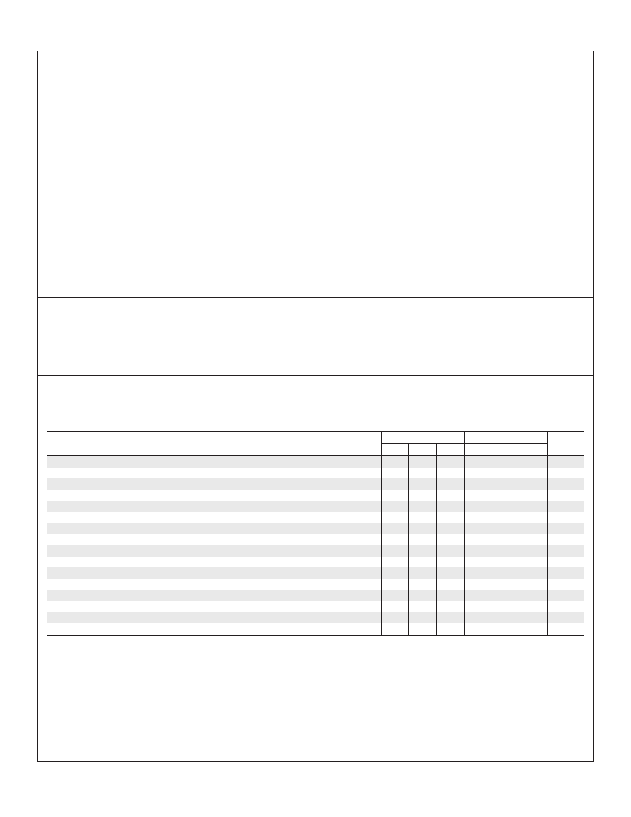
ELECTRICAL CHARACTERISTICS
(Unless otherwise specified, these specifications apply over the operating ambient temperatures for SG109 with -55°C ≤ TA ≤ 150°C, SG309 with
0°C ≤
T
A
≤ 125°C,
and
for
V
IN
=
10V,
I
OUT
=
500mA
(K,
R,
and
IG
-Power
Packages-)
and
I
OUT
=
100mA
(T-package).
Low
duty
cycle
pulse
testing
techniques
are used which maintains junction and case temperatures equal to the ambient temperature.)
Parameter
Test Conditions
Output Voltage
Line Regulation
Load Regulation
Total Output Voltage Tolerance
Quiescent Current
Quiescent Current Change
Output Noise Voltage
Long Term Stability
Ripple Rejection
TA = 25°C
VIN = 7.1V to 25V, TA = 25°C
TA = 25°C
Power Pkgs: IOUT = 5mA to 1.5A
T-package: IOUT =5mA to 500mA
VIN= 7.4V to 25V
Power Pkgs: IOUT = 5mA to 1.0A,
P ≤ 20W
T-package: IOUT =5mA to 200mA, P ≤ 20W
VIN = 7.4V to 25V
With Line : VIN = 7.4V to 25V
With Load: Power Pkgs: IOUT = 5mA to 1.0A
T-package: I =5mA to 200mA
OUT
f = 10Hz to 100KHz, TA = 25°C
T = 25°C
A
SG109
SG309
Min. Typ. Max. Min. Typ. Max.
4.7 5.05 5.3 4.8 5.05 5.2
4.0 50
4.0 50
Units
V
mV
15 100
15 50
15 100 mV
15 50 mV
4.6 5.0 5.4 4.75 5.00 5.25 V
4.6 5.0 5.4 4.75 5.00 5.25 V
10
10 mA
0.5
0.5 mA
0.8
0.8 mA
0.8
0.8 mA
40
40
µV
10
20
mV
50
50
dB
4/90 Rev 1.1 2/94
Copyright © 1994
LINFINITY Microelectronics Inc.
11861 Western Avenue ∞ Garden Grove, CA 92841
2
(714) 898-8121 ∞ FAX: (714) 893-2570
Share Link: 