ST485BD 데이터 시트보기 (PDF) - STMicroelectronics
부품명
상세내역
제조사
ST485BD Datasheet PDF : 19 Pages
| |||
Electrical characteristics
ST485
4.2
Receiver switching characteristics
VCC = 5V ± 5%, TA = TMIN to TMAX , unless otherwise specified. Typical values are referred
to TA = 25°C)
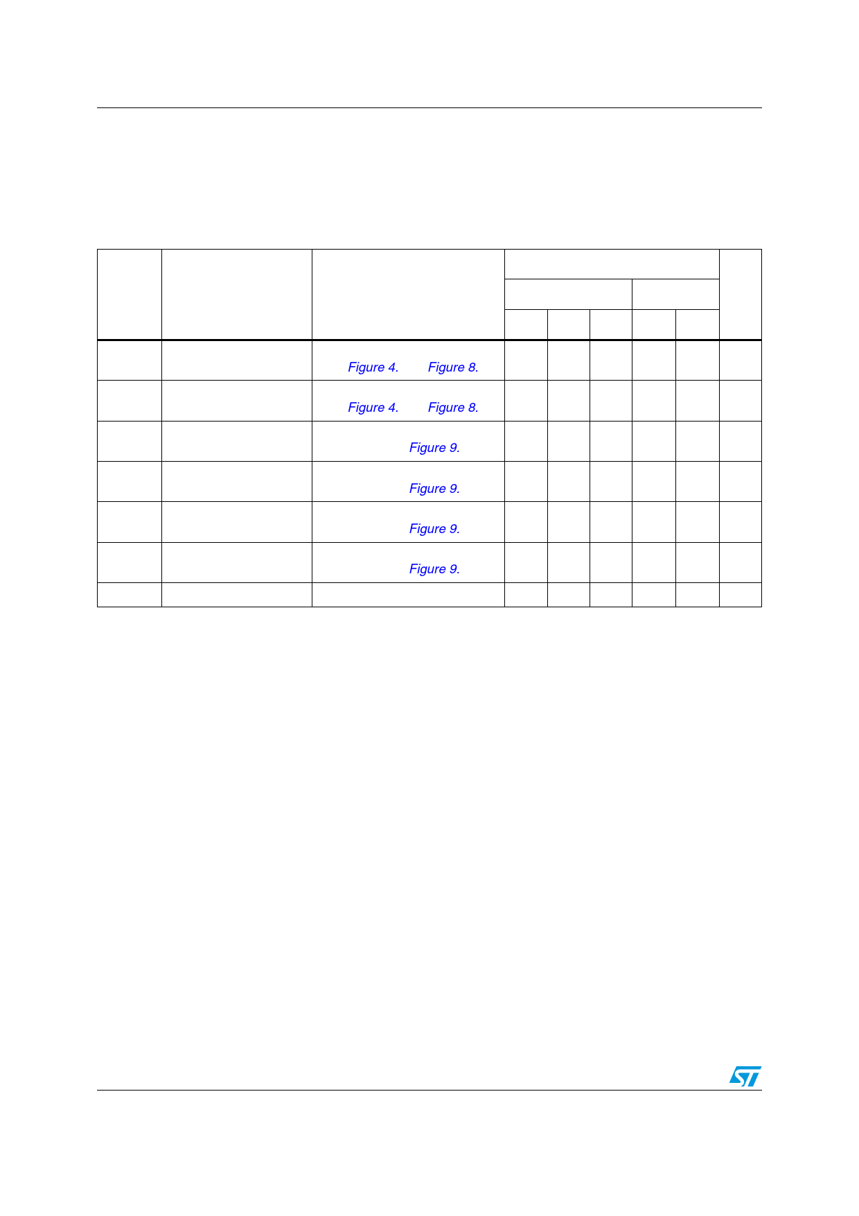
Table 7. Receiver switching characteristics
Symbol
Parameter
Test conditions (1)
Value
-40 to 85 °C
-55 to 125°C Unit
Min. Typ. Max. Min. Max.
tPLH
tPHL
Propagation Delay Input RDIFF = 54ΩCL1 = CL2 = 100pF
to Output
(See Figure 4. and Figure 8.)
20
130 210
tSKD
Differential Receiver
Skew
RDIFF = 54ΩCL1 = CL2 = 100pF
(See Figure 4. and Figure 8.)
13
230 ns
ns
tPZH Output Enable Time
tPZL Output Enable Time
tPLZ Output Disable Time
tPHZ Output Disable Time
CRL = 15pFS1 = Closed
(See Fig. 2 and Figure 9.)
CRL = 15pFS2 = Closed
(See Fig. 2 and Figure 9.)
CRL = 15pFS1 = Closed
(See Fig. 2 and Figure 9.)
CRL = 15pFS2 = Closed
(See Fig. 2 and Figure 9.)
20 50
20 50
20 50
20 50
56 ns
56 ns
56 ns
56 ns
fMAX Maximum Data Rate
2.5
2.5
Mbps
1. All currents into device pins are positive; all cuttents out of device pins are negative; all voltages are referenced to device
ground unless specified
8/19
Share Link: 