ST75C176CN(2006) 데이터 시트보기 (PDF) - STMicroelectronics
부품명
상세내역
제조사
ST75C176CN Datasheet PDF : 18 Pages
| |||
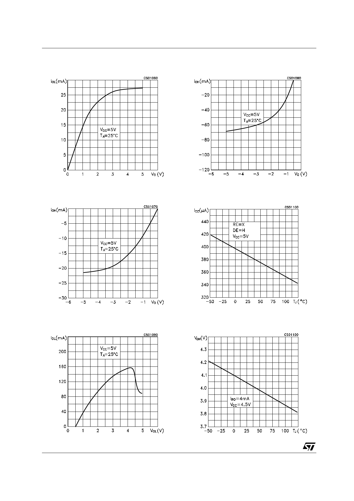
Electrical characteristics
ST75C176
Table 7.
Symbol
Receiver switching characteristics
(VCC = 5V ± 5%, TA = TMIN to TMAX, unless otherwise specified. Typical values are referred
to TA = 25°C) (See Note 1)
Parameter
Test Conditions
Min. Typ. Max. Unit
tPLH
tPHL
tSKD
tPZH
tPZL
tPLZ
tPHZ
fMAX
Propagation delay input to RDIFF = 54Ω, CL1 = CL2 = 100pF
output
(See Figure 4 and Figure 8)
Differential receiver skew
RDIFF = 54Ω, CL1 = CL2 = 100pF
(See Figure 4 and Figure 8)
Output enable time
CRL = 15pF, S1 = Closed
(See Figure 3 and Figure 9)
Output enable time
CRL = 15pF, S2 = Closed
(See Figure 3 and Figure 9)
Output disable time
CRL = 15pF, S1 = Closed
(See Figure 3 and Figure 9)
Output disable time
CRL = 15pF, S2 = Closed
(See Figure 3 and Figure 9)
Maximum data rate
20 130 210 ns
13
ns
20
50
ns
20
50
ns
20
50
ns
20
50
ns
2.5
Mbps
Note:
All currents into device pins are positive; all cuts out of device pins are negative; all
voltages are referenced to device ground unless specified.
8/18
Share Link: 