STK16C68 데이터 시트보기 (PDF) - Unspecified
부품명
상세내역
제조사
STK16C68 Datasheet PDF : 9 Pages
| |||
STK16C68
1. Read address
2. Read address
3. Read address
4. Read address
5. Read address
6. Read address
0000 (hex)
1555 (hex)
0AAA (hex)
1FFF (hex)
10F0 (hex)
0F0F (hex)
Valid READ
Valid READ
Valid READ
Valid READ
Valid READ
Initiate STORE cycle
The software sequence must be clocked with E
controlled READs.
Once the sixth address in the sequence has been
entered, the STORE cycle will commence and the
chip will be disabled. It is important that READ
cycles and not WRITE cycles be used in the
sequence, although it is not necessary that G be
low for the sequence to be valid. After the tSTORE
cycle time has been fulfilled, the SRAM will again be
activated for READ and WRITE operation.
SOFTWARE NONVOLATILE RECALL
A software RECALL cycle is initiated with a
sequence of READ operations in a manner similar
to the software STORE initiation. To initiate the
RECALL cycle, the following sequence of READ
operations must be performed:
1. Read address
2. Read address
3. Read address
4. Read address
5. Read address
6. Read address
0000 (hex)
1555 (hex)
0AAA (hex)
1FFF (hex)
10F0 (hex)
0F0E (hex)
Valid READ
Valid READ
Valid READ
Valid READ
Valid READ
Initiate RECALL cycle
Internally, RECALL is a two-step procedure. First,
the SRAM data is cleared, and second, the nonvola-
100
tile information is transferred into the SRAM cells.
After the tRECALL cycle time the SRAM will once again
be ready for READ and WRITE operations. The
RECALL operation in no way alters the data in the
EEPROM cells. The nonvolatile data can be recalled
an unlimited number of times.
HARDWARE PROTECT
The STK16C68 offers hardware protection against
inadvertent STORE operation and SRAM WRITEs
during low-voltage conditions. When VCC < VSWITCH,
software STORE operations and SRAM WRITEs are
inhibited.
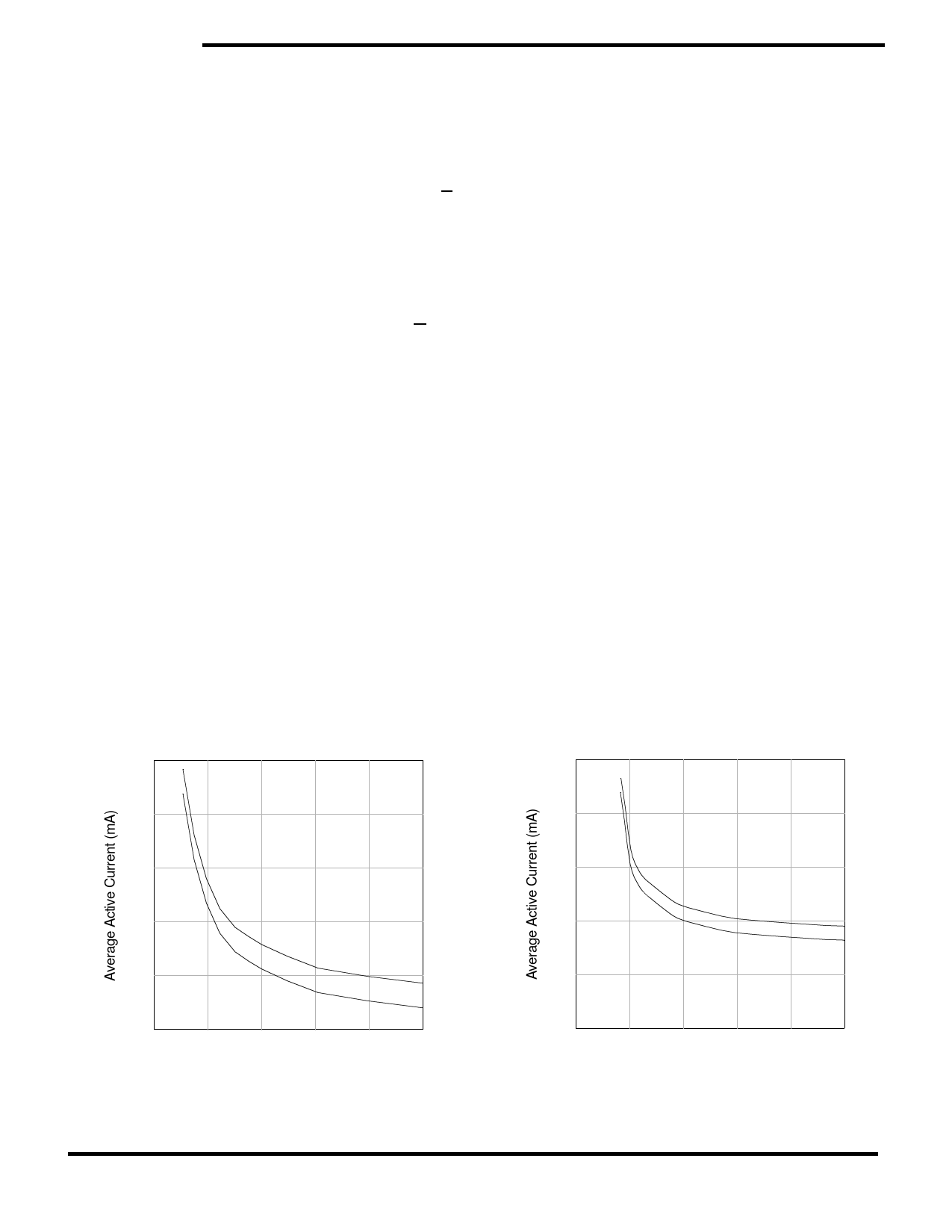
LOW AVERAGE ACTIVE POWER
The STK16C68 draws significantly less current
when it is cycled at times longer than 50ns. Figure 2
shows the relationship between ICC and READ cycle
time. Worst-case current consumption is shown for
both CMOS and TTL input levels (commercial tem-
perature range, VCC = 5.5V, 100% duty cycle on
chip enable). Figure 3 shows the same relationship
for WRITE cycles. If the chip enable duty cycle is
less than 100%, only standby current is drawn
when the chip is disabled. The overall average cur-
rent drawn by the STK16C68 depends on the fol-
lowing items: 1) CMOS vs. TTL input levels; 2) the
duty cycle of chip enable; 3) the overall cycle rate
for accesses; 4) the ratio of READs to WRITEs; 5)
the operating temperature; 6) the VCC level; and 7) I/
O loading.
100
80
80
60
40
TTL
20
CMOS
0
50
100 150 200
Cycle Time (ns)
Figure 2: ICC (max) Reads
60
TTL
40
CMOS
20
0
50
100 150 200
Cycle Time (ns)
Figure 3: ICC (max) Writes
July 1999
4-80
Share Link: 