TA2125AF 데이터 시트보기 (PDF) - Toshiba
부품명
상세내역
제조사
TA2125AF Datasheet PDF : 7 Pages
| |||
TA2125AF
Precaution Use
(4ch BTL)
• Input stage
Minimum input DC voltage range for buffer is 0.2 V
• Driver stage
Each channel driver consists of BTL configuration linear amplifier.
Voltage gain is fixed: Gv = 15.2dB
• VCIN terminal
VCIN is reference voltage terminal for input signal
• GND
Pin 8~10 and Pin 27~29 are connected to FIN through inner lead frame.
Each FIN are not connected each other also.
The heat of power dissipation is transferred to PCB, through PW-GND Pin. PW GND is connected to substrate
of Pellet to connected copper foil area as large as possible.
• VCC1/VCC2
Pin 14 and pin 23 are not connected through AL layer on chip.
(H-Bridge)
• VR/VM terminal
VR terminal is control for H-brige dynamic range. I36 = 30 mA (Brake Mode)
VM terminal is VCC terminal for H-Bridge.
• STBY/REG STBY
STBY is standby control terminal for 4ch BTL.
REG STBY is standby control terminal for regulator.
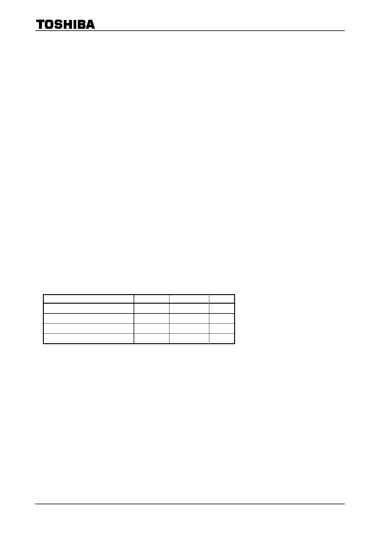
Maximum Ratings (Ta = 25°C)
Characteristics
Supply voltage
Power dissipation
Operating temperature
Storage temperature
Symbol
VCC
PD
Topr
Tstg
Rating
12
1.7
−35~85
−55~150
Unit
V
W
°C
°C
3
2003-10-07
Share Link: 