TCL1117 데이터 시트보기 (PDF) - TelCom Semiconductor, Inc
부품명
상세내역
제조사
TCL1117
TelCom Semiconductor, Inc

TCL1117 Datasheet PDF : 9 Pages
| |||
800mA LOW DROPOUT POSITIVE REGULATORS
ADJUSTABLE AND FIXED 2.85V, 3.30V, 5.00V
PRELIMINARY INFORMATION
TCL1117
TCL1117-2.85
TCL1117-3.30
TCL1117-5.00
APPLICATIONS
Overload Protection
The TCL1117 is protected against current (short-circuit)
and thermal overload conditions. Thermal protection is
triggered by a chip temperature exceeding 165°C. Current
overload is triggered at approximately 950mA.
Stability and Load Regulation
The TCL1117 requires a capacitor from VOUT to GND to
provide compensation feedback to the internal gain stage.
This is to ensure stability at the output terminal. Typically, a
10µF tantalum or 50µF aluminum electrolytic is sufficient.
NOTE: It is important that the ESR for this capacitor does not
exceed 0.5Ω.
The output capacitor does not have a theoretical upper
limit and increasing its value will increase stability.
COUT = 100µF or more is typical for high current regulator
designs. NOTE: See Protection Diodes for limitations. An-
other benefit of larger output capacitance is improved tran-
sient load response (large di/dt in the load).
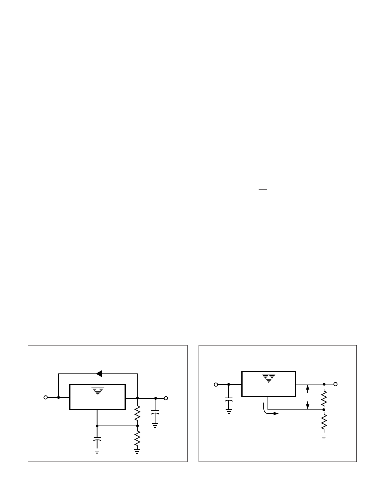
Protection Diodes
Typically no protection diodes are necessary for the
TCL1117. Unlike older regulators, the ADJ pin is protected
internally from excessive currents. The ADJ pin can be
driven with voltage transients as high as ±25V with respect
to the output without damage to the device.
Likewise, a diode between the input and output is not
typically required. If the input voltage collapses the internal
circuitry can absorb ~20A transient currents (<10µsec)
without damage. This reverse current is much larger than
most power supply designs can generate. However, if the
output capacitor is VERY large (>1000µF), instantaneous
currents can be high enough to damage the chip. In this
case, a high-current, fast-response diode is recommended.
(See Figure 1).
Output Voltage Adjust
Like most LDOs, the TCL1117 regulates the output by
comparing the output voltage, or a multiple thereof, to an
internally generated reference voltage. On the adjustable
version, the VREF is available externally as 1.25V (±1%)
between VOUT and ADJ (See Figure 2). The voltage divider
formed by R1 and R2 should be set to conduct 10mA
(minimum output load). The output voltage is given by the
following equation:
( ) VOUT = VREF 1+ R2 + IADJ R2
R1
On fixed voltage versions of the TCL1117, the voltage
divider is provided internally.
Load Regulation
The TCL1117 load regulation is limited by the resistance
of the wire connecting it to the load (Rp, Figure 3). For the
adjustable version, the best load regulation is accomplished
when the top of the resistor divider (R1) is connected directly
to the output pin of the TCL1117, NOT to the high side of the
load (Figure 3). When so connected, Rp is not multiplied by
the divider ratio. For the fixed output versions, the top of R1
is internally connected to the output and the ground pin can
be connected to the low side of the load as a negative side
sense if, so desired.
D1
1N4002
(OPTIONAL)
VIN
IN TCL1117 OUT
VOUT
VIN
IN TCL1117 OUT
VOUT
ADJ
+
R1
COUT
150µF
ADJ
IADJ
50µA
VREF
R1
+ CADJ
R2
10µF
R2
( ) VOUT = VREF
1+ R2
R1
+ IADJ R2
TCL1117-05 6/5/97
Figure 1.
Figure 2. Basic Adjustable Regulator
3
Share Link: