TK65010 데이터 시트보기 (PDF) - Toko America Inc
부품명
상세내역
제조사
TK65010 Datasheet PDF : 8 Pages
| |||
TK65010
THEORY OF OPERATION
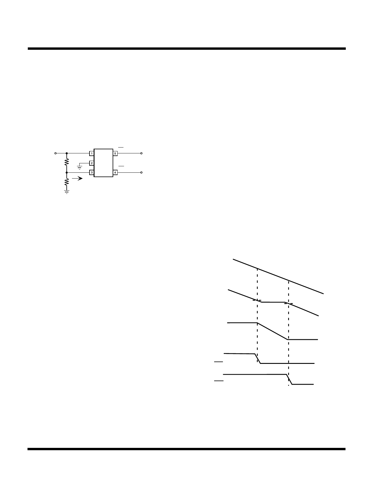
The circuit in Figure 1 illustrates a typical application
utilizing the TK65010. The TK65010 differs from most
voltage monitors due to the fact that two separate
comparator thresholds can be set utilizing a single resistive
divider and a single input pin. One comparator output is
used as an early “low battery” warning. The second
comparator can be used as a later “dead battery” warning.
BATTERY IN
R1
301 K
R2
1M
VIN
GND
VMON
IFB
LBO
DBO
LOW BATTERY
DEAD BATTERY
FIGURE 1
Under these conditions, current will be flowing into the
VMON pin and will be limited to approximately 580 nA. As
the battery voltage drops, the voltage on the VMON pin will
drop proportionately. When the voltage on the VMON pin
passes through approximately 710 mV, the output of the
first comparator (LBO) will transition from a high to a low
state. Shortly after the LBO output has been asserted, as
the input voltage continues to drop, the magnitude of the
current into the VMON pin will begin to proportionately
decrease as the input voltage decreases. An op-amp
feedback loop internal to the TK65010 will attempt to
maintain the voltage on the VMON pin at a constant value of
approximately 700 mV (thus, the plateau). As the battery
voltage continues to drop, there comes a point where the
feedback current decreases to approximately zero. A this
point, the voltage on the VMON pin will resume a proportional
drop with the input voltage. As the voltage on the VMON pin
passes through approximately 690 mV, the second
comparator output (DBO) will be asserted.
In a typical voltage monitor, which uses an external resistive
divider for setting the voltage monitor threshold, the input
bias current to the monitor pin is essentially zero. In this
type of scenario, the voltage on the monitor input would be
a resistively divided version of the battery voltage. The
TK65010 introduces a small feedback current (IFB) which
introduces a “plateau” into the transfer characteristics
between the battery voltage and the voltage monitoring
pin. The width of this plateau is dependent upon the current
range of the feedback current (IFB) and the values of the
external resistor network. Figure 2 illustrates the typical
relationship between the battery voltage (VIN), the feedback
current (IFB) and the voltage on the monitoring pin (VMON).
In selecting a resistor divider network, there are typically
two degrees of freedom when selecting values. The first
criteria in selecting the divider is the ratio of the two
resistors. Selecting the ratio defines the lower threshold of
the voltage monitor (DBO). The second degree of freedom
when selecting the resistor divider is the absolute resistance
values. This second degree of freedom can be utilized to
set a secondary monitoring threshold (LBO) greater than
the first.
For details on how to properly select the resistor divider,
refer to the “Design Considerations” section.
VLBO
VIN
VDBO
VMON
580 nA
IFB
700 mV
0 nA
LBO
DBO
Typically, when the battery voltage is relatively high, the
voltage on the VMON pin of the TK65010 will be a resistively
divided version of the battery voltage minus the offset. The
magnitude of the offset voltage will be dependent upon the
resistor values comprising the external divider and the
magnitude of the feedback current flowing into the IFB pin.
FIGURE 2
January 1999 TOKO, Inc.
Page 3
Share Link: 